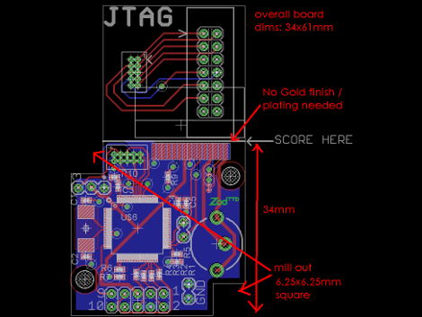
[Colin] has cut his teeth with about fifteen PCB orders. He wrote a tutorial describing the process and sharing his tips on avoiding common problems. You may remember our own How-To prepare designs for manufacture early last year. In that post, [Ian] shared his veteran knowledge by outlining BatchPCB’s board design process. This time, [Colin] is using Advanced Circuits in Colorado as a board house, giving us more insight on how the different companies work. No matter who you choose for manufacturing, make sure you really understand how to properly format and troubleshoot your designs. It’ll end up saving you a lot of time and money.


Good tutorial, though funny to think of cutting your teeth on fifteen orders though! That’s the number of PCBs I’ve ordered over the course of the past year, but good stuff anyway.
The only thing I wish you could do from Eagle for Advanced Circuits was specify how to scale the drill file. Maybe 3 times out of every 4 they misscale the drill file and I get a million “missing soldermask” violations about 12 inches away from the edge of my board.
One more thing you should always do for Adv. Circuits: if it’s a multi-layer board, GIVE THEM A LAYER STACKUP! They want to have a file which confirms which layers go where, what they mean (especially if you included a lot of “Drawing/Other” files).
The article is very nice, but I don’t agree with something: “Print out a 1:1 ratio copy and compare it with any parts you already have stock of. This is a little over the top, but a nice sanity check.” This is very important: I always print a 1:1 copy and stick all connectors in the paper. This way I can see if I can really mount that heatsink, if I can put a ribbon cable in the connector, etc.
I do my own boards on my CNC, but I still do a lot of checks before, because paper is cheaper than PCB+mills+4 hours wait time :)
Just to make it clear: I don’t agree with the fact that he says it’s over the top. I consider it a necessity :)
I’m 100% in agreement with Fili.
I’ve seen numerous PCBs that failed this one aspect of design. And it’s a royal pain to have connectors on stubby wired because they don’t fit in the allowed space.
I bet the professionals don’t need to do this, but I sure do.
33$ a board (doesnt mention how big that is) with a min order of 4, yea I would print it out on paper at least once before sending in that 100$
I guess here is as good a place as any. Have any of you guys tried out http://www.pcbwing.com? It seems their prototype pcb option is a pretty decent deal. It’s not a huge amount of money to spend on a trial order but it’d be nice to hear if someone had tried them out before and what your experience was.
As we already are talking about PCB-design: Can anyone help me with the design of the AVRISP Arduino shield? I took the EAGLE files to my work, because we have a small PCB-drill (one of those little CAM machines)…but after the PCB was done and i took a look at it, i noticed, that the traces and especially holes were way too small. They weren’t just too small to solder…like 2/3 of the board was short-circuit.
Do i need to redesign the AVRISP-Board, or did i just make something wrong?
It’s well worth it to find one non-electronic device if you make PCB’s – a small electric tile cutter with a diamond wheel – [I was lucky enough to fine one for $10 at a garage sale] – its much nicer than using a jig saw or such to cut the boards apart (very nice staight lines) They go thru PCB stock like a hot knife thru butter, and when you have 60 sq inches to play with for a PCB layout and pay only $50 extra for multi-up its well worth it to pay the extra $50 and load your layout with multiple patterns or combine several different PBCs on the one panel –
@Nomad tough to say whats wrong without more info, could be lots of things.
I tried batchpcb and I was pretty happy with it, wasn’t a huge fuss at all. Advanced circuits is a bit fussier.
i might have a try with silver circuits after a recommendation though
http://www.custompcb.com/
@charliex: Sorry i’ve forgot to paste the link to the page: http://drug123.org.ua/mega-isp-shield/
I don’t have more information about the drill, but i think theres no problem getting that from the right person. I’ll ask around if necessary.
Good comments – I agree with the printing out of boards to trial fit new parts prior to sending out to fab. Also, I would add to that sanity checking parts you haven’t used before with gerber visualisation tools. Altium is really nice for this because you can get an actual 3D render of your board – great for seeing where you’ve forgotten to put an aperture in your solder mask… which I actually got caught out on with the boards I -just- got back… sigh… Fortunately, nothing some time with a hobby knife can’t fit.
I hope Eagle gets a 3D board visualisation tool like Altium!
@Paul: Well at least there’s Eagle3D:
http://www.matwei.de/doku.php?id=en:eagle3d:eagle3d
I’m guessing the library isn’t quite up to the standard and size of Altium’s but then again it’s $0 vs $XXk so…
Coppercam is pretty useful as well, my cnc uses PhCNC which is also very good for verifying.
@Nomad i meant more info on what went wrong, i can cnc that board, but my cnc does like 6mil no problem.
Agreed Altium is an amazing software package. I understand its out of the price range of many hobbyists but being able to import the package for a product from solidworks and mate it with the PCB, complete with 3D models of all components is such and insanely useful tool. If it stops you from one or two failed prototype enclosure fabrications or PCB runs it has paid for itself.
The Dorkbot group here in Portland OR has a guy who runs a group PCB buy every 2 weeks. He’s had to switch away from Advanced Circuits recently due to cost, but the design rules are still the same: 6mil trace/space, 13mil min drill. The order is open to anybody (in the US, I assume).
Boards are $5 per square inch for 3 copies, any shape within reason. Art deadline is 8am every other Monday (yesterday was the most recent), and boards arrive by the next Wednesday (used to be Monday, but new board house is slower).
http://www.dorkbotpdx.org/wiki/pcb_order
Working on a commercial prototype I have to say this order has saved me countless hours and probably over $1000 just in the last month or so. The 2-week cycle of order, populate, redo, order, rinse repeat is ideal. If there’s enough interest outside of Portland I’d love to see it become a weekly order ;-)
Also, he’s looking at doing a 4-layer order as well, but it depends on both the current 2-layer boards being a little more popular, and there being enough interest in 4-layer ($10/sqin for the same 3 boards).
@charliex: I’ve placed two orders with Silver Circuits, one turned out really well, the other is still on it’s way but I don’t expect any problems. They’re pretty responsive, even though they’re 12 time zones away from me. Tough to beat their prices on little two-layer boards.
My recommendation goes out to sunstone.com. Cheap protos, they run all kinds of deals (free electrical test, double order, etc.) DFM, you name it. One of the best thing though is that they take Eagle files directly!
No connection, just a satisfied customer.
Also… check out gerbmerge… something many people don’t know is that you tend to pay roughly the same amount of money for 1 board or 10 if they all fit in a panel. Gerbmerge is a little python script that fits any number of boards into a given panel. I was able to triple my board count for my last order and added only $100 to the price. This helped bring my per-board cost down.
I have used Advanced several times also. But for small quantities the total order always is about $500. Have been using recently pcb-pool.com. Most everything I do is SMT and they are currently shipping a free solder paste stencil with most sample orders.
@Dielectric cool . thanks for the reference on it, i think i’ll give em a go on my next run
eagle has a panelise thing
http://www.neufeld.newton.ks.us/electronics/?page_id=81
@charliex: As i said before, the drilled board wasn’t only too hard to solder, because the copper around the holes was not wide enough (some of the holes even collapsed), but 2/3 of the traces were shorted.
I tried rescuing the board with a really thin knife, but after that, the board didn’t look so good anymore…and this didn’t fix the soldering problem…it even made it worse.
PS: Could we continue this via E-Mail or on an IRC-Server (preferably mine)?
@nomad I’m usually lurking on efnet in nsl
I have been using FreePCB for my board layouts. It’s a great little Open Source program. It’s very easy to use. The hardest part for me when first learning was figuring out how to export a PADs netlist from orcad. Have you guys tried FreePCB? I wish more developers were involved to iron out some of the minor quirks that it has.
@nomad sorry i was afk for a while there but i saw the pictures.
to me it looks like a couple of problems, drill bits used were too large for the vias ( or the via’s werent big enough ) I usually oversize the via’s a bit for cnc’ing, eagle does this in the DRC.
secondly the pcb cutter looks ok, but it looks like there was no rubout isolation done, which is removing all the copper that needs to be removed between the tracks, that’d be the shorts.
finally use some of the scotch red scrubbing pad gently to remove the swarf, just be careful and don’t remvoe tracks.
Advanced circuits does their 5 boards for $133 all day long. Great price for professional boards. You can also get them up to something like 90 sq inches (can’t remember), and you can also “step-repeat” (get more than 5 boards, for an addition $50 (mean, fill in the entire 90 square inches per board, of board space.
To comment on sneakypoo’s posts regarding pcbwing — I gave them a try as their pricing is very very attractive. However, I will not order from them again. The customer support is non-existent and on top of that I received my order about 1 1/2 weeks late in a paper bag . . .
Go to http://www.protoexpress.com/betterdfm/index.jsp for free DFM.
I tried batchpcb and I was pretty happy with it, wasn’t a huge fuss at all. Advanced circuits is a bit fussier.
i might have a try with silver circuits after a recommendation though
http://www.4pcbassembly.com
I try rushpcb http://www.rushpcb.co.uk they offer best price and also design pcb.
I hope there price is best one from all.
Recently I tried FASTBOM http://fastbom.com, a startup based in China providing low-priced PCB services for from prototype, production to turn-key requirements. To date, everything goes well.
I set Seeed Studio Fusion https://www.seeedstudio.com/fusion_pcb.html as my default pcb manufacturer