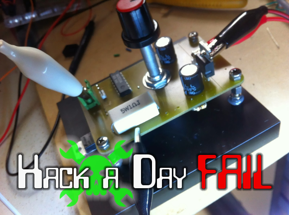
When [Simon] fried his 3A rated FET with just 500mA of current he wrote it off to an inability of the SOT23 package to dissipate the heat without a heatsink. For the next iteration of the project he upgraded to a 12A rated part. Luckily he decided to test the circuit one more time before sending his board off for fab. He threw together this constant current load test which led him to discover his failure.
The switching circuit, which was for his home security system project that we’ve seen at least twice, worked just fine up to 500mA. But when he drove it above that threshold the package quickly warmed up. It got so hot that it actually reflowed its solder joints! The problem has to do with oscillation, but even with further testing he couldn’t get the FET to reliably shut off all the way. Take a look at his fail write-up linked at the top and then let us know some possible remedies for the situation.
 Fail of the Week is a Hackaday column which runs every Wednesday. Help keep the fun rolling by writing about your past failures and sending us a link to the story — or sending in links to fail write ups you find in your Internet travels.


Interesting writeup. One minor thing though- I highly recommend avoiding four-way junctions in schematics. Altium in particular has an issue where one of the four wires can be 0.00001 mils off grid from the other three wires, and not be connected. The difference is small enough that it will be covered by the junction dot. Similar things can happen with manual junctions as well as imported schematics. When junctions are limited to three wires, there is never any doubt.
There’s nothing to fix. He built a linear regulator, and was surprised that it works like a linear regulator. There’s no simple solution to fix that problem, because it involves building a whole switching mode regulator with feedback.
What he actually wanted is just a fast fuse.
Although thinking out of the box, he could add a thermistor and a piece of metal to the FET, and use a comparator circuit to cut the current completely when the FET starts to warm up. The circuit would immediately limit the current to 500 mA and then cut off if the short circuit doesn’t go away.
The piece of metal would act as a heat mass, which slows down the oscillation period to a second or so, which means the circuit will tolerate a short output surge, and also auto-reset.
There also very temperature sensors. e.g. Microchip MCP9501 – 9504 that are self contained and gives you a digital output when it exceeds a factor preset temperature.
Well there you have it. Put a logical high on the FET’s gate when the heatsink’s temperature exceeds 85 C and it turns off for a few seconds due to the hysteresis.
Exactly this. He built a linear regulator, which means that once the current surpasses the set point, that FET has to dissipate any additional power. The circuit is DESIGNED to make that FET get hot.
tekkieneet’s answer below explains the oscillations. There’s a large capacitance (the gate) in the feedback loop.
– If you want a circuit breaker, you want to latch and shutdown when OC.
The MOSFET should be either on or off, so the heat dissipation is
minimum. You can use a dual comparator and use the spare one to make a
latch. Play with spice (e.g. LTSpice) to test your idea.
There is also the trick of using a LDO regulator as an OC protection and
it comes with its own current sensing and thermal protection!
– Bad practice to drive a MOSFET directly from opamp. Large MOSFET has
lot of capacitance and regular opamp does not like to drive large
capacitive loads. Opamps go into instability/oscillation because of
phrase issues. If you must, either use one that is designed for
driving large cap load and/or use a series resistor on the MOSFET gate.
For MOSFET the “Input capacitance” (CISS) parameter is pretty much self
explanatory. You have to factor in Millers effects (CRSS), CISS would
at least give you some idea of the order of magnitude you are dealing
with.
His oscillation issue is that the FET is acting as an amplifier. Driving two amplifiers in a feedback loop without compensation is inherently unstable regardless of load and will give oscillations.
The unstable loop isn’t why it was burning hot though.
In National version of the LM324 datasheet (LM324-N on TI’s site). TI’s
own version doesn’t have apps example nor go into detail like Nation’s.
Capacitive loads which are applied directly to the output of the
amplifier reduce the loop stability margin. Values of 50pF can be
accommodated using the worst-case non-inverting unity gain connection.
Large closed loop gains or resistive isolation should be used if larger
load capacitance must be driven by the amplifier.
MTP3055: Ciss 410pF (typ) 500 pF (max) and is directly driven by LM324
which is spec to only 50pF of capacitive load. It sis driven WITHOUT a
series resistor in the constant current circuit.
Heat problem is the “breaker” that acts like a linear circuit i.e.
constant current source instead of latching On/Off as I have stated.
Also might want a small series resistance on the transistor base. If
there is a short, until the transistor/MOSFET reacts, the BE junction
can see huge current.
Here is my idea for a cheapo fuse assuming that your 15V is regulated.
The circuit would trip when it sees an OC, but will come back a few
moment later. It will oscillate at low duty cycle if the output is dead
shorted, but your MOSFET would be either On or Off to minimize power
dissipation.
Use a TL7702B (TI) Power supply supervisor to replace your transistor.
Sense the voltage after your resistor. When that voltage drops below a
threshold due to IR drop, the RESET pin 6 will go high pulling your PMOS
off. You can program the threshold with a voltage divider on the SENSE
pin. After a programmable amount of time (programmable by CT), the
circuit will reset itself. Make sure you add a series resistor to CT per
datasheet as you would want a very large CT.
The TL7702B works up to 18V, output well defined down to 1V, comes
with an internal reference + comparator, time delay and 2 output
polarities.
put a 100nF cap between souse and gate…
The heating isn’t due to oscillation – at least, it needn’t be. When he hits the current limit, the FET’s resistance increases to keep the current at the limiting value. It doesn’t switch off because there’s no switching circuit here – only linear feedback. This is exactly how a constant current load works (like, say, my Re:load!).
An alternative might be using an opamp as a comparator to enable a latch (which could be made with another opamp or an OR gate) which disables the FET – but for speed you’re not going to beat something actually designed to be a fuse.
(non-EE here)
“But unfortunately the drain – source resistance is now significant and losses in the MOSFET cause it to heat. At 15V and 500mA the MOSFET is dissipating 7 1/2 Watts.”
Is this something that is not factored into the maximum switching frequency?
getting a higher current rated part wont change its heat distribution …
[Quote]
When [Simon] fried his 3A rated FET with just 500mA of current he wrote it off to an inability of the SOT23 package to dissipate the heat without a heatsink.
[/Quote]
He didn’t use a heatsink, and wonders why it failled… hmm? what could be the problem.
I know: use a heatsink…
I would add, read the datasheet before.
Even a small FET can switch far more current than this without a heatsink. It’s only an issue if (as this one did) they go into linear mode.
I’m really glad that Simon shared his writeup. I could just as easily see myself letting something like that slip through, so I’m glad his experience has become my experience. Plus One!
Nothing starts off complicated but if you pursue it things can get complicated.
I agree with Dax. He built a linear regulator – and an unstable one, at that. Below the regulation point, the FET is full on and happily dissipating minimum power. Above the regulation point, VGS is reduced until the on resistance of the FET increases to absorb the extra power, heating as physics dictates.
As a side note, this type of instability is common with LDOs, which is why it is important to read through the manual to see if a minimum input or output capacitance is required for stability.
The only (thermally) cool solution is a current-mode (or voltage-mode with current limiting) switching regulator. On a more detailed note, you also need to make sure that your regulator has sufficient feedback network bandwidth so that it is fast enough to catch the smallest surge that you want to filter.
I don’t understand the approach here. Why use a MOSFET for a linear regulator? MOSFETS have a very low ‘on’ resistance which makes them ideal for switching regulators but they also are easy to drive ‘on’ and hard to drive ‘off’ which can lead to oscillations, high dissipation etc. Bipolars are better for linear regs. I think MOSFETS are overused because they (in some situations) work more like an ‘ideal’ transistor in that, you don’t need to worry so much about the non-ideal properties of a real transistor such as the voltage drop Vbe or capacitance Cbe, Cec and Hfe etc. MOSFETs eliminate some bipolar problems in some situations but they can introduce some other (MOSFET) problems to replace them. I think the bottom line is to understand the ways in which transistors are ‘not’ ideal and design accordingly.
Thanks for sharing.
To meet the author’s goal of fusing with high accuracy, they just need to add a comparator with enough positive feedback to latch up. This will keep the FET out of the linear regime. If the author really wants a constant current/constant voltage type of behavior, then you’re stuck with either huge heatsinks (think TO-3 parts…) or a switching regulator design. A third option would be to build a “crowbar” circuit in conjunction with the author’s original polyfuse to trip it at a defined setpoint by dropping a short (the proverbial crowbar) across the polyfuse.
I also forgot to add that you need to select linear-rated FETs or go with BJT due to the positive feedback issues that switching FETs typically experience at these dissipation levels.
There a couple of problems here.
The first is the low side current regulator. While conceptually this is a simple circuit, there can be problems one of which is oscillation. That is easily prevented by rolling off the gain of the opamp using a capacitor (10nF or so) between the output and non-inverting input.
The other is using yet another current regulator circuit on the high side when what is needed is an electronic fuse. A couple of seconds work (searching for “electronic fuse”) turned up a simple circuit using a TRIAC. An SCR would probably work as well.
It’s NOT a Wednesday! Plus the author discovered the difficulty so it’s a wonderful learning experience doggedly progressing towards eventual accomplishment. It’s not like burning down the ham shack when that new 1kw linear final melted the antenna because the swr was a bit off. Ahhh… but then again the subject is a FAIL… not DISASTER.
Am loving the wealth of experience being voiced here, thanks guys.
Needs to replace the PNP transistor with a PNP NPN pair configured as an SCR and add a 1K to 10K resistor between the current shunt ant the PNP gate. Many BEAM solar engines use circuits like this. http://www.beam-online.com/Robots/Circuits/1381.html Then, as long as his FET is “off” with -1.4Vgs the circuit will latch off cleanly. He’ll also be able to add a reset button that connects the NPN’s gate to ground with a 1K ohm resistor.
Get rid of U2A and run the prior op amp straight into the MOSFET gate. Adjust source resistor as needed for the current you want. Deal with the power due to dropping voltage across the MOSFET (times the current)
Will someone please post a schematic of what would, in their opinion, work best for this scenario? There are a bunch of what seem like great/good explanations/fixes in the comments, but for some reason I’m really having trouble filtering them down into a useful circuit/idea. Apparently my inner visual learner is driving my brain car right now and my written-word learner is tied up and chloroformed in the trunk…
Please and thank you!
*Wait* for Simon to test/sort out the ideas and copy a working design from him.
As others have pointed out, gate capacitance is a big problem with FETs. I had a co-op job in college where we were investigating FET failures in a PWM circuit running a large inductive load. The engineer who designed the circuit was more in love with his design than he was in actually fixing the problem. His solution was to put in a much larger FET, thinking that it would be able to handle the the gate noise better.
The lesson here is that a bigger FET also has a much larger gate which in turn creates a larger capacitance between the gate, drain, and source. The 1KHz switching signal easily fed back into the gate drive circuit and made the FET fail much more quickly. I produced spice models demonstrating the problem, but no one would listen to me.
I never did find out what their solution was, but I’m thinking they probably changed over to a transistor based circuit.