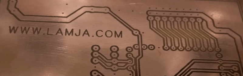
There are dozens of circuit board printers out there that lay down traces of conductive ink and ask you to glue down components to a fragile circuit board. This is a far cry from the old way of making PCBs, but these printers are going gangbusters, cashing in on the recent popularity of hardware startups and rapid prototyping.
People who think deeply about a problem are few and far between, but lucky for us [Arvid] is one of them. He’s come up with a way of creating PCBs with any 3D printer and steel rod. The results are better than anything you could make with a circuit board printer, and the technique is very, very cheap.
[Arvid] is using the traditional method of etching away copper, just some ferric chloride and a bit of time. How he’s masking the copper that shouldn’t be etched away is a unique process we haven’t seen before. He’s simply covering a piece of copper clad board with permanent marker, and scribing the parts he wants to be etched with a sharp steel rod attached to a 3D printer.
The G code for the printer was generated by FlatCAM, a piece of software made specifically for cutting PCBs with a mill. [Arvid]’s technique works so well that spindles and mills aren’t needed; only a sufficiently sharp instrument to scrape away permanent marker.
Thanks [Hassi] for sending this one in.


It’s nice. However I have never been able to find a permanent marker that can resist ferric chloride. I often use a marker to cover pieces of copper that are outside of the main board area to save some etchant, but it always ends up eaten away.
I never tried ferric chloride because of its nasty staining properties.
I had a great success with sodium persulfate, also known as B327. To me, any waterproof marker is an unpenetrable barrier. I use that to fix bad spots after toner transfer, works great.
If you’re just saving etchant (which I wouldn’t bother, mine is $5/kg, which lasts for a few hundred boards) then try masking the areas with regular tape.
Yes, I actually use tape.
so do I & with ferric chloride
I use an ordinary CD marker. The key to etchant resistance is to heat up your PCB after drawing with a halogen lamp or a hairdryer. Ever since I started to use this method, there is no overetchingon my boards.
Other than that, I (and almost all my colleagues in Poland) use sodium persulfate. Much cleaner and supposedly gives better results.
^This. It doesn’t take long for paint to dry to the touch, but it may take days or even weeks at room temperature for it to dry completely and reach full strength. Heat accelerates this greatly. I put the PCB with in an oven preheated to 250°F for 30-60 minutes.
Acrylic paint (the type that artists use) makes a great resist when heat treated in this manner. So will most other paints too, I just favor acrylic since it’s cheap, doesn’t have nasty fumes or overspray, and cleans up with water prior to drying. For covering large areas of PCB that you don’t want etched, it’s much easier than going over the area with a permanent marker. I don’t know if it would cut away cleanly with a scribe, might be worth trying.
And always make sure the copper is properly prepped before applying any resist. Clean and roughed up.
I’m not sure why people are so insistent about roughing up their copper surface before applying any masks.
It may seem counter intuitive, but the best surface to start etching on is a perfectly clean surface that’s best achieved with a smooth copper surface. The surface must be wettable as possible, and even something as common as cleaning the surface with alcohol can affect this negatively. The best way to prepare a smooth copper surface is to scrub it thoroughly with a cleaning product like ajax and rinse clean with clean water (ideally deionised).
A ready surface will not have water bead on its surface, but instead the water will spread and wet the surface. This allows optimal adhesion between any mask and between the uncovered copper and etchant solution.
This is good info. I polish PCB material with 600-grit sandpaper to remove any surface corrosion, almost to a mirror-finish, and get excellent toner adhesion. I’m sure if the surface is smooth to start with, any mild abrasive like kitchen cleanser or toothpaste is all that’s needed. I don’t think the conventional wisdom of using brillo or other rough abrasive pads is actually helpful.
I also find that 600-grit brush finish facilitates acceptable transfer to brass, aluminum, and stainless steel. Only mirror-finish stainless has defeated my toner transfer attempts so far.
A surface needs a little microscopic “tooth” for good adhesion. You don’t want it perfectly smooth, nor to have deep gouges. It doesn’t appear you realize it, but you actually ARE roughing up the surface by using Ajax – which contains crystalline silica!
I’ve used polishing paste (for car paint) on one board. Result – perfect 7mils traces and rather good 5 mils with toner transfer. I can’t go lower because of printer dpi. Surface was then cleaned with soap, there was very good wetting.
I use ammonia solution, it makes toner adhesion very reliable.
I do not use persulfate because it produces cavitation and cavitation can damage resist. UV resist not so much, but toner tends to break away quickly. Besides one batch of FeCl lasts me years (I do not etch very often) and is always ready, just put it in a hot water bath for speed. Persulfate works only once, maybe twice if you were generous.
As for curing the marker ink by heat, good idea, may be worth trying for some quick and dirty 60s looking PCB with funny traces.
Have you tried something like “machinist’s blue” or DYKEM or one of the products in that space?
http://www.grainger.com/product/DYKEM-Blue-Layout-Fluid-2C945
Readily available, and it’s very low viscosity, so it’s easy to spread. It might not hold up to the etchant solution at all, though.
For the occasional rework on toner transfer, I’ve found that sharpie works great. Use the black one and it seems fine. (One of the few cases where I’d recommend the particular brand, as some other similar markers haven’t worked.)
I found that “varnish” markers works the best :)
These markers use Nitrocellulose lacquers instead of alcohol. You can discern it by your smell ;)
The idea of applying an even coat of resist and then selectively scratching it away with a sharp stick puts me in mind of the wax tablets they used to use in ancient Rome. They were wood or stone with a thin layer of contrasting wax on top which they’d scratch away with a stylus. I wonder if the right wax would make a decent resist for this machine to scratch off?
Try the common Edding 400 permanent black marker
I use fine-tip paint pens. These are fine enough to touch up 16mil traces if you have a steady hand:
http://www.sharpie.com/enus/pages/oil-based-paint-marker.aspx
The paint resists ferric chloride indefinitely (until undercutting). I remove it with acetone or brake parts cleaner.
Spray Paint and a laser cutter is similar to this method…
Yes, but you could build an entire 3D printer/CNC plotter in the price of just a laser suitable for general-purpose laser cutter.
and should not be done. At least not with the normal CO² cutters. Those emit infrared light and copper is highly reflective to infrared afaik. So burning the paint on copper with a CO² laser will reflect and damage the optics.
I wonder if this work for SMD stuff. Would be a good alternative to milling if it would do sub-mm pitch.
This is a cool hack, but if you’re going to do chemical etch anyway, you might as well do the UV photoresist. You can either use the tried and true transparency mask or a little UV laser. The UV laser could easily extracted from a bluray drive and mounted on this modified 3D printer.
UV laser is not as simple as it sounds. Out-of-the-box it might be good for low-resolution boards (think 16 mil traces). I’m actively trying and didn’t have much success so far (although I’m keeping the cost down as a priority and want to re-use as much as possible)
The blu-ray drive is designed for extremely close working distance (the distance between the lens and the disk), in order of 0.2mm. Add half the thickness of the lens and you get focal length of roughly 1mm. This means if you mess up the focus (or worse – the planarity) by just 0.5mm, the laser spot will be ~1mm instead of much desired ~0.1mm.
I’m working on using the focus error signal from the bluray pickup head’s photodetectors to find the exact distance between the lens and the surface of the PCB. From there, I can control the voice coil motor in the drive to set exact beam size.
I expect there are more problems to come, such as beam profile (laser power vs angle is not a brick wall function, but rather a bell curve), dimensional repeatability (needed to align 2 or more PCB layers) etc.
An easier way would be to remove the laser from the drive and mount it in a quality collimator lens. This however is far more expensive than my budget and has some drawbacks (such as inability to change spot diameter, therefore requiring high linear feed rates to maintain constant exposure energy per unit of area)
This sounds like a terrific project. Please publicize your results when you’re ready.
I don’t fully understand the need for variable spot diameter you mention in your last paragraph, but I wonder if you’ve considered driving the diode at different power levels for the same variable exposure effect with fixed focus. This is how any high-speed diode modulation application works (laser printers, fiber optic links). Simply switching the diode on and off is very bad for lifespan, since it’s harder to control current transients.
I evaluated the AD9660 for a laser data link using this principal, many years ago. Unfortunately it’s long since out of production. I’m sure any laser printer uses something similar that could be salvaged.
Meh, it was done before many times. Linear feed machines, laser printer mirror scanners, galvo scanners, you name it.
As nobody ever opensourced their setups, I might publish when I get meaningful results ;)
@Modulation
Yes, modulation is absolutely necessary to prevent overexposure of surrounding areas while using a tight spot. I’m struggling to find a decent laser driver that doesn’t cost a fortune and has a high power output (fiber applications – ~100mW, my needs – ~500mW peak). After all, I might resort to a DIY programmable constant current source modulated with a mosfet. I’m more a software/digital guy, so It’d be a mystical adventure into the world of unstable feedback loops and magic smoke :D
@Spot size
From my rough estimates, If I were to keep spot size at a constant 100um, 100mW laser would require 100cm/s feed rate and total exposure time will be ~5 minutes for eurocard-sized board coated with a typical photoresist material.
My crude ex-printer CNC setup achieves only 30cm/s peak, so we’d get 3x over-exposure and wasted laser power. Also, 15 minutes instead of 5.
And remember, the goal of my project is to reuse useless crap, buying brand new optics to collimate doesn’t count ;) Therefore to use the stock bluray pickup head reliably, we should do the auto-focusing anyway because of the aforementioned short focal length and impractically tight tolerances.
I decided to conserve the printer mechanics, the laser and my patience, choosing lower feed rates.
If we program the g-code to expose filled areas, for example ground planes with a larger spot, feed rates of 15cm/s at 500-1000mW are possible, optimistically reducing the time 15-fold.
Alternatively, I might use a second voice coil motor (the one the drive uses to accurately lock on a track on a wobbly high-rpm CD). That would reduce required feed rates 6-10 fold.
I also evaluated other options, such as laser printer. These are even worse, requiring complex optics for precision work. The optics included in original hardware are unsuitable because of poor UV handling capability. Low-divergence collimator or galvo prices – don’t event ask.
Hi Matt,
¿Which pickup are you using?
We already do that using the PHR-803T optical pickup. We hacked the device (see here for info – http://www.diyouware.com/node/161) and now we control almost 90% of it. We can turn on/off the diodes, control the power, read the photodiode array, control de servos and of course focus the laser using the astigmatic method through the photodiode A,B,C,D signals. We use the IR laser to focus to avoid blurring the film. Then we switch to the blu-ray diode to draw the PCB. About over-exposuring the surronding areas actually we use solar-film to protect the photoresist from excess light but we are researching other methods.
Actually we are printing at 600DPI. It means the dot size is approx. 40 micrometers. Really is not a dot because the pickup split the main beam in three beams to provides a tracking mechanism.
We developed all the electronics, the software and two PCB printers with it.
All are open-source projects so you can obtain all the information at our site:
http://www.diyouware.com/
Hi Victor,
Thanks for sharing your experience. Good reverse engineering.
I haven’t purchased the pickup head yet, but I was planning on getting something like SF-BW512L due to its high power capability. Since you pointed out the issues with the beam profile, I’m more skeptical now. I think pickup heads with recording capability should have better optics, otherwise written disks would be dodgy on low-cost drives.
Your 3-legged table fixture is a pretty nice idea. Does this motion system have a special name? What are the benefits of using this method instead of the classic 3 linear planes?
Hi Matt,
@ SF-BW512L
I don’t know the device but usually they use a diffration granting in front of the laser diode to split the beam. It is easy to remove it from there. Once removed you will have only the main beam. But really the beam dot is so tiny that for most applications is better to use the three. Even unfocus a litle the beam to have a bigger dot. Anyway main problem you will have is to find the pickup pinout to obtain the photodiode signals and implement the code to focus the lens. It’s not imposible but take a lot of time. In our case almost a year.
@Your 3-legged table fixture
The name of this configuration is inverted delta. Main advantage is that simplify the design if you want to move a small working piece using diferent heavy tools. Also it isolate the laser beam from motor vibrations which really was the reason we adopted. It also allows to interchange tools easlily which is very important for a multi-functional printer.
Good luck with your project! Keep us informed.
Also, I failed to mention that you get the variable spot size FOR FREE with no extra hardware. Because the allowable wobble of the BD-ROM exceeds the working distance (0.2mm vs 0.6mm) you have a large amount of adjustment available. One can get a ~1um spot size (fully in focus, at physical constraints) up to ~6mm (basically one third magnification).
I’m still waiting for my quality laser goggles, can’t wait to test that.
Also forgot to mention: unlike other methods, such as cutting/3d printing/toner transfer, LDI hash more uses in PCB prototyping:
– Paints for soldermask or silkscreen are UV-curable. You could mill the paint but it’s not as elegant or reliable as not putting it in the first place.
– There are dry film photoresists that can be used as cover during selective via electroplating or to cover drilled and metallized vias during etching.
My long term goal is in-house low-cost rapid (<1 day, not 1 week plus China shipping) prototyping of functional 4+ layered boards.
I’ve gotten pretty good results with a laser.. https://hackaday.io/project/3904-tonerless-pcb-etch-resist-direct-to-pcb-method
Can you share your experience? What setup did you use and how were the results in comparison with other methods?
Cutting adhesive material didn’t work for me because the laser was melting the material too much and distorting fine details. I got similar results as toner transfer, which was not worth the effort for me. Regarding the photo methods, I also tried professional CtF masks – great results up to 5-6 mil but you need an exposure box and DTP shops are rarely available.
For what I’ve done so far (still a work in progress) I use a shapeoko2, I started with a small 450nm 100mw laser that I got on eBay for about $15.. I moved to a 1watt laser which allows me to cut a lot faster.. I’ve been using Eagle then I import the .brd into Chilipeppr.. I’m hoping Chilipeppr moves on to allowing you to select the board level, but for now it requires a little effort.. and to toggle the laser, I wrote a python script that adds the commands.. I’ve had some great success with pretty fine pitch as you might see in the pics on the project page.. I haven’t had much time lately, but I am pretty positive it can do better still. As for the melting, I haven’t had any trouble whatsoever with the vinyl I’ve been using.. I use the craft vinyl that is meant for signmaking that you can buy on amazon, etc.. I tried MANY other things and it works the absolute best…and black vinyl works better than others, although the orange works really well with the 405nm laser.. The only issue I can think to mention is a slight residue from the adhesive sometimes which can be removed very easily with a wipe and some alcohol…definitely don’t use acetone on the vinyl..the alcohol works very well.. I’m trying to keep the project page as current as I can.. There’s a couple other related projects I have going that include UV exposure as well…. (all in various states of progress)
https://hackaday.io/project/4565-tonerless-pcb-templates-for-uv-exposure
https://hackaday.io/project/3787-diy-uv-exposure-oven-for-pcb-etching-and-masks
https://hackaday.io/project/3905-tonerless-pcb-etch-resist-uv-exposure-method
https://hackaday.io/project/3903-small-pcb-chemical-etching-machine
https://hackaday.io/project/3785-diy-metal-pcb-solder-paste-stencils
So … could you use something like a lightscribe drive and a CD-shaped board covered in resist to just directly do the printing, and then straight into the etchant? Or if you could get enough control over the encoding and bits going onto the underside of the disc, and use the actual BD diode …
I could see a next level hack. Can we just shape our board like a dvd and put it in a dvdr or lightscribe drive and burn it there? I dont know how hard would it be to get the drive to forego the disc test and stuff, but the hardware is pertty awesome and incredibly cheap!
Quite creative. I thought the ink would chip away and create overetches. There is some irregularity, but not bad. I wonder if it would be possible to v-groove using that thing.
Too bad the author posted so little info. For such a simple board, toner thermal transfer or even photolitography with homebrew inkjet films would’ve been much faster and not require dedicated hardware. Speaking of dedicated hardware, recently I’ve been working on laser direct imaging of a photoresist for making my PCB’s. Having achieved reliable 6-7 mil with toner transfer, I think it should be possible to prototype boards with 3/3 mil traces cheaply using LDI.
Nice !. i’ve used a similar method , it’s gives a prety good results :
https://www.youtube.com/watch?v=enHj1F4HRbQ
I used to do something similar with machinists blue and an old pen plotter with a sharpened screw threaded into the remains of a pen. It was slow and loud, but did very neat boards. It’s cool to see an updated version of this!
Not quite what I was expecting. Does anybody know if PLA or ABS can resist ferric chloride?
I’ve been wondering about printing directly on to a copper clad board, one or two layers thick.
Yup, should work fine.
http://www.plasticsintl.com/plastics_chemical_resistence_chart.html
that would work, but the traces would also be quite thick.
Here’s my attempt at the same thing using a nail in a Cricut machine from a few years back: http://everhack.blog.atxhackerspace.org/2011/03/29/pcb-process-update/
“How he’s masking the copper that shouldn’t be etched away is a unique process we haven’t seen before.”
I’ve seen it before. Maybe not in the last year or two, and on HAD. But this technique goes way back. Folks used to do this with plotters and spring-loaded scribes. The resist most commonly used was lacquer, IIRC.
Yep. a cheap pen plotter and a nail or scribe and you spray the board with lacquer.
Built one back in the early 90’s. the blue toner sheets are massively easier to use and laser printers are basically free nowdays.
When I use a laser engraver for my boards (laser is at work, wish I had one at home) I use the 99 cent flat black spray enamel from walmart, cheap, dries in like 5 min and engraves cleanly. When I have to do a simple board and not wanting to wait to go back to work I will use the same stuff and a scribe point in a xacto knife for the same effect
Interesting technique. The best etchant mask I have ever found – that resists everything from ferric chloride up to HCL&H202 – is a can of white Rustoleum spray paint. For fine stuff, “spread and bake” T-shirt silkscreen ink works wonders.
Sorry for what I’ll wrote, but this method wear the 3D printer and it’s the step of inking the board its unnecessary, I’ve done this very simple, this way: output the Eagle File to an PNG or antother image you can import in openscad, select milimeter as scale, import the image to openscad and then EXTRUDE it exatly the vertical (Z axis) resolution of your printer, need no more than that, then put the cleaned board on the 3D printer Bed, callibrate height and “3D” print the circuit board (the printer wil deposit PLA on the traces and everywhere you need), then go to the ferrum cloride bath step, once removed the unecessary copper, clean the board and remove the PLA with acetone, and you get an board quickier and more precise trace than with this method, not wearing the printer, not modding the printer etc, I’ve used this apporach with common PLA printer and resin, just select the rigth PLA/Resin resitent to ferrum cloride.
Interesting.. What trace widths do you get with that method? What’s your printer’s nozzle diameter?
0.3 mm wide traces are possible better at 0.6 mm if your pinter has ,3mm xy resolution, of course depends on your printer capabilities, resin printers are limited by the projector resolution, but use to be much better.
I really wanted to try this myself, but never got the time. Can you post some pictures and more details about it?
Maybe next time I need an PCB, by now I’m very busy on other projects.
I always use enamel paint to resist ferric chloride etching. Works like a charm. The biggest problem with this method is painting on the PCB pattern with a fine artists brush. I have pondered about alternate ways of printing enamel paint on the PCB pattern but cannot think of an easy/cheap way of doing so. This method might be the solution to that. Coating the copper clad board with enamel paint and scraping it off according to the PCB pattern. I’m guessing enamel paint would scrape off easier than permanent marker as it has sort of a latex like consistency when its dry.
that’s what I do, spray the board with some 99 cent fast dry and scribe (or laser engrave), works great
I don’t see anything new. it’s even on the wikipedia https://en.wikipedia.org/wiki/Aquatint
This technique was used with acid and rosin by artist since middle age.
Awesome! Now what’s the cheapest 3D printer around to start out with this?
I’ll admit to being dumb and that I don’t work with electronics so don’t hate on me to much for my stupid question.
Would it be possible to use a process like this on a CD? I don’t know how viable the aluminum in CDs are for making complex circuits but certainly a CD seems like it has potential for producing very cheap boards, even if you have to deposit the copper on the disc yourself. If aluminum is all that’s necessary it also seems like it would be even cheaper since the etching chemicals wouldn’t need to be as potent to etch away such a thin layer of material.
This isn’t a stupid question. It’s close to brilliant. But there are serious problems.
You wouldn’t be able to solder to the CD without melting the polycarbonate substrate (and probably vaporizing the aluminum coating). Soldering to aluminum is problematic anyway, since it’s such an active metal. You would need to use conductive ink or glue instead.
The aluminum layer is extremely thin (~50nm). You can even see through it. Conductivity would be poor. Power handling capacity would be negligible.
There might be niche applications where CD-based PCB would be useful. Capacitive touchpad?
how about etching a cheap inductive “fuse” using a CD? paint the data side with conductive ink and tool-etch the coils on both sides. since the conductive properties of aluminum are so poor it would protect more sensitive electronics from voltage spikes. better the magic smoke comes from a recycled CD than a $14 fpga, rite?
Here’s a known niche app using similar process/materials. Etch a pattern onto aluminized mylar, which then serves as both coil and diaphragm in a planar magnetic tweeter. Like you say, power handling is low, although the incredibly low mass is claimed to make it very responsive.
As for actual CDs, capacitive touchpads are a good idea. Fractal antennae come to mind as another possible niche app. Thin aluminum isn’t the best material for that, but I wouldn’t be surprised if it still performed well. Would also look cool if displayed prominently.
I’ve heard that FeCl reacts much faster with aluminum than copper. Typically described as “violently”, or some similar adjective; resulting in boiling, steaming, spattering, rapid resist undercutting, and other things you don’t want FeCl doing. Have never tried it to verify, but on the first attempt, it may be a good idea to start with highly dilute FeCl.