Work on HaDge – the Hackaday con badge, continues in bits and spurts, and we’ve had some good progress in recent weeks. HaDge will be one conference badge to use at all conferences, capable of communicating between badges.
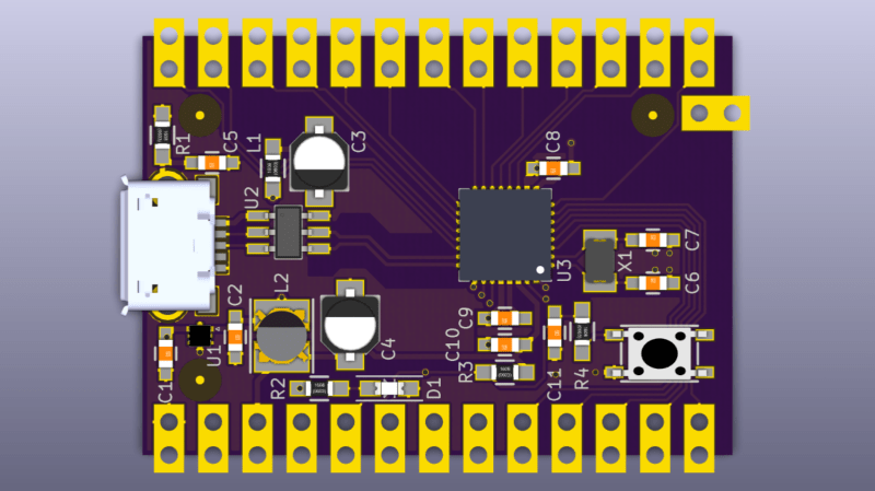
Picking up from where we left off last time, we had agreed to base it around the Atmel D21, a 32-bit ARM Cortex M0+ processor. To get some prototype boards built to help with software development, we decided to finish designing the HACK before tackling HaDge. HACK is a project that [Michele Perla] started that we have sort of assimilated to act as the prototyping platform for HaDge. We wanted a compact micro-controller board and hence opted for the SAM D21E – a 32 pin package with 26 IO’s.
[Michele Perla] had earlier designed HACK based on the larger 32 pin SAM D21G and used Eagle to 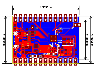 draw the schematic and layout. Using the Eagle to KiCad script, he quickly converted the project and got on to making the board layout. I took up the rear guard, and worked on making his schematic (pdf) “pretty” and building up a schematic library of symbols. While [Michele] finished off the board layout, I worked on collecting STEP models for the various footprints we would be using, most of which I could get via 3dcontentcentral.com. The few I couldn’t were built from scratch using FreeCAD. The STEP models were converted to VRML using FreeCAD. Using [Maurice]’s KiCad Stepup script, we were able to obtain a complete STEP model of the HACK board.
HACK is now ready to go for board fabrication and assembly. We plan to get about 20 boards made and hand them out to developers for working on the software. The GitHub repository has all the current files for those who’d like to take a look – it includes the KiCad source files, PDFs, gerbers, data sheets and images. The board will be breadboard compatible and also have castellated pads to allow it to be soldered directly as a module. Let us know via group messaging on the HACK project page if you’d like to get involved with either the software or hardware development of HaDge.
In a forthcoming post, we’ll put out ideas on how we plan to take forward HaDge now that HACK is complete. Stay tuned.


USB spec mentions that your inrush total should be less than 50uC… that’s gonna be very tough to respect with these 2x10uF + 2×2.2uF caps…
Definitely overkill on the 10ufs. The chip doesn’t even have wifi, no reason it should need that much bypass power.
It seems like using free software makes everything more difficult. Don’t get me wrong, I’m super grateful that free software exists, but you could do everything within Altium if you had a license (though I’ve only every used circuit maker from altium, I suppose the real thing is better)
The main goal was to be made with free software so it would be hackable and diy at home.There might also be some other problems regarding licenses if\probably Hackaday is going to sell this.
Yeah, I understand that, but it must be frustrating to use all kinds of interfacing scripts between software packages and whatnot. I’m glad Hackaday and other groups use free software or people like me would have no way of reproducing/modifying/contributing because we don’t have access to the big software packages they use in industry. I’m sure it’s not uncommon to use 5 or more software packages to design a single project. I’ve used LTspice, eagle, diptrace, autoCAD (via student license), and code composer studio on really simple projects. If money was no object I could have gotten away with one or two packages probably.
We did just fine with mooltipass….
Now here’s an idea! Make it so HACK and Mooltipass can be connected together!
B^)
This design was done in the free version of Eagle, which prohibits commercial use, so it’s legally questionable for Hackaday to distribute these PCBs as part of a paid conference (or really, for anything other than strict personal use).
I have no idea why this wasn’t just done in Altium CircuitMaker. It’s totally free (as in beer), and there’s no restrictions on designs. Automatically in the cloud, version-controlled, and supports teams.
Reading this post is absolutely hilarious. They make it sound like a huge freaking deal to do this design and integrate 3D models into it. I could lay this board out in about 20 minutes in CircuitMaker, with 3D models and all. Sometimes I forget how terrible other PCB packages are.
This project was originally designed in Eagle, that’s true, but then it was TOTALLY redesigned in KiCAD; after all, I found it easier to just remake the board from the ground up. Plus, we made several layouts (first with SAM R21G and PCB antenna, then with D21G and integrated RF Module) before this final one.
PS: this layout was done in circa 1 working day; optimization, footprints checks, parts sourcing, and reiterating on these steps took most of the time.
PPS: this project is being developed in free time (as in “I’m at work and I have 5 spare minutes” or in “I could sleep one hour less today”)
I find sillier to have to roll up your own components on proprietary tools.
“I have no idea why this wasn’t just done in Altium CircuitMaker.”
I’d be pretty dubious about using CircuitMaker for any of my own projects. That would be based on Dave Jones’ reports of it losing data (due to issues saving local data to the cloud). And the fact that it’s totally cloud based, meaning that they could potentially hold my data hostage. It doesn’t seem like a forgone conclusion to use CircuitMaker…
Kicad has its faults, and Altium Designer is not doubt a more complete product. But Kicad works reasonably well for projects like this, and its free (as in freedom and beer).
Early, early alpha/beta versions of CircuitMaker had some funny issues, but I never had any files disappear. It’s now out of public beta and in its first release version. I’d definitely check it out.
Your files are stored in the cloud, but they’re checked out locally to your AppData folder. If the internet explodes, you can still open your CircuitMaker projects by dragging them into the program. It’s really not as big of a deal as people are making.
Because CircuitMaker is a closed-source, cut-down, shitty program. Everything that’s “in the cloud” is unreliable and useless, because its function depends on the Altium servers.
Beer isn’t free – you pay for it by submitting your body to Bill Cosby (excuse crude humor, no such thing as a free lunch). KiCAD by comparison is an awesome program with autorouting built in, bazillions of modules available online and 3D built in. It can even export to about 45 different formats (while CircuitMaker can do 4 or so IIRC).
KiCAD is way more lightweight as well, last time I tried installing Altium it used up (with minimal install) 7 freaking gigabytes.
i agree, developing better free softwares that would tend toward an Altium design environment type would further improve the development of free hardware designs.
Hey there. Why is the ground plane moved away from the USB traces?
Because whoever laid this out is pretending they’re doing impedance-controlled differential stripline layout. But with a two-layer board like this, they’d have to use a super-thin board thickness (<0.1 mm?) to get those 6 mil traces to hit 45 ohm single-ended impedance referenced to ground. The whole board layout is pretty ridiculous.
Also there’s only one ground pin on the perimeter. One! The design could stick VDDA at the edge but not another ground pin to go with it? I don’t want to have to build adapter boards to go with the dev board, much easier to hang hacks off a badge with plentiful ground/power pins.
Does anybody know if OSH Park can make boards with through-hole pads cut in half by the board outline?
I did it. They do. But I’m not sure if they’re happy with that in general, they might not get the same results every time from different board houses.
Thanks. I don’t have any immediate application, but it might come in handy sometime.
Yes they sure can – this was done some time ago https://goo.gl/qoj6d8
Thank you.
Interesting, not sure how it’s a badge (no display or LEDs?) but it’s also very obviously a noob layout/schematic. Try making it with toner transfer, then revise and have it fabbed professionally. Don’t waste money making YADevelopmentBoard that nobody is going to use after some conference.