We return once again to the work of Dr. Claude E. Shannon, this time to his Masters thesis on relay switching circuit design. This thesis introduced switching algebra that allows the systematic design and optimization of logical circuits. While Shannon’s work applied to switches and relays, it is equally applicable to all the modern forms of digital circuits. His thesis received widespread notice when published as “A Symbolic Analysis of Relay and Switching Circuits” in 1938. This work built on the Boolean algebra developed by George Boole and an analysis of logic by Augustus De Morgan which these mathematicians published nearly simultaneously in 1847. To some extent, it was the beginning of the age of modern digital logic.
Basic Rules
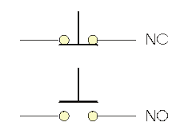
Switching algebra is easily visualized using switches since there are only two values: on and off, or true and false. In digital systems we represent these as 1 and 0, respectively. There are only two rules which create the basis of the algebra. The first rule is the NOT operation, or negation. Mathematically this is:

Physically, a normally open (NO) switch and a normally closed (NC) switch are the negations of one another. When a NO switch is represented by the symbol X, a NC switch would be represented as X’, where the apostrophe indicates the negation.
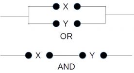
The second rule can be expressed in two different ways. One form is the AND operation, or conjunction, while the other is the OR, or disjunction. Formally these operations are:

![]() The switch diagrams help clarify these rules but we’ll switch to logic gates now to use a more modern representation.
The switch diagrams help clarify these rules but we’ll switch to logic gates now to use a more modern representation.
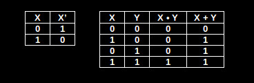
Truth tables are a representation that defines the operation of a system. This truth table demonstrates how AND and OR are related since if you negate one of the columns and flip it top to bottom you get the values in the other. The formal expression of this relationship is:
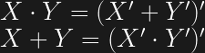
Since each of these operations can be derived from one another, only one is needed as the second rule in the switching algebra. The AND and OR operators, represented by ‘•’ and ‘+’, are analogous to multiplication and addition and they follow the same rules for commutation, association and distribution. Note that just as we often omit the multiplication operator in arithmetic, the AND operator can also be omitted by concatenating the variables used in the expressions. Here is the math showing the relationship between these operations:

One of the goals of the switching algebra is to use math to reduce circuits, represented by expressions, to their simplest or, in some cases, a form using specific logic gates. There are math identities and simplification rules that designers can use to accomplish this refactoring.
The algebraic identities that can be used in refactoring are:

Here are some simplification rules useful in refactoring:

The final important consideration is the order of precedence for operations. Again, they are similar to regular arithmetic:
- Left-to-right
- Complement (NOT)
- AND
- OR
The order of precedence is less well defined for logic circuits, like XOR or NAND, which are derived from the three basic circuits. It is best to use parenthesis to clarify the order of operations when using these operations.
Using Boolean algebra as switching algebra, complex circuits are expressed so that they can be evaluated mathematically. This quickly increased the productivity of the engineers designing switching circuits, some of which were being used in computers.
Half Adder
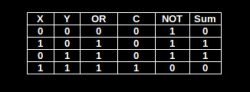
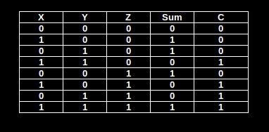
Let’s apply switching algebra to the design of a half adder, a core circuit in CPUs. 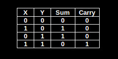 A half adder takes two binary inputs and generates two outputs. One output is the sum of the inputs while the other is a carry to the next stage. The truth table shows the desired outputs.
The carry output is obviously an AND of the two inputs. That makes the design easy.
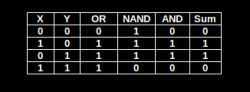
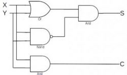
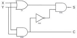
The sum can be generated in a few different ways depending on the circuits the designer wants to use. Let’s look at one approach using OR, NAND, and AND gates. A truth table with columns for each step helps the analysis. The OR column shows the results of that operation on X and Y. Next is the result of a NAND on X and Y. The final column is an AND of the OR and NAND columns which produces the desired sum output.
We can express this mathematically as:

We can simplify the circuit by refactoring the math to reuse C to calculate S. To do this, the NAND is removed and the output of C negated by a NOT gate passed as an input to the final AND of the circuit. The half adder now is:
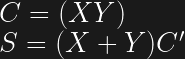
We can reduce the gate count considerably by introducing an XOR gate to directly provide the summing operation. The XOR operation is represented by the math symbol ‘⊕’ in equations. The half adder now uses only 2 gates and appears mathematically as:
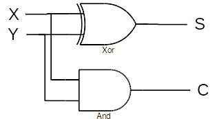

These different implementations of a half-adder illustrate the trade-offs made during circuit design. Integrated circuits contain multiple gates of a type, say NAND gates. If you have free gates in an IC using them for a circuit instead of adding another IC, like an XOR, saves money and board space in a design.
Full Adder and Karnaugh Maps
A useful design tool is the Karnaugh Map developed by Maurice Karnaugh in 1953. This map is another form of truth table that is useful for extracting the math relationships among the input and output values. The table is constructed by listing input values along the top and left axis with the output values in the body of the table. We’ll use maps to design a full adder with more rigor than used designing the half adder.
A full adder has the same two X and Y inputs but also an input carry, Cin, sent from the previous stage. The outputs are the same, the sum, S, and the output carry, C. For convenience and to eliminate confusion between the two carries we’ll represent Cin by Z in this analysis.
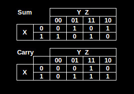
With the truth table defined we can construct two Karnaugh Maps, one for the sum and the other for the carry. The X values run down the left side while across the top are the Y and Z values. Notice that the values for Y and Z are in the order 00, 01, 11, 10 (0, 1, 3, 2). When multiple inputs are listed the sequence can only change one bit for each column or row. This is called a Gray code.
The body of the map is filled by copying the resultant values for the inputs. For example, in the sum map when X = 1, Y = 0, and Z = 1 the result is 0. The carry result for the same inputs is 1.
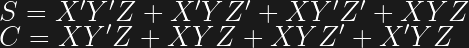
To begin the mathematical analysis we write the boolean expressions for the cells that contain a 1. Using the same X, Y, Z values of 1, 0, and 1 we write an expression for this cell because the result in the carry table is 1. We don’t write an expression for the sum table because its cell is 0. The sub-expressions for each table’s cells are combined with an OR into an expression for each table. The expressions for the sum and carry are:
Focusing on the sum, the refactoring begins by factoring out X’ from the first two sub-expressions:

Next, based on reference materials, we know that the expression (Y’Z + YZ’) is an XOR of Y and Z. Making that change and factoring out X in the last two sub-expressions we get:

Again based on references, we know that (Y’Z’ + YZ) is an equivalence, a logical operation we don’t normally use. Its value is 1 when the operands are equal, which is the negation of XOR which is 1 when the operands are unequal. The next two steps refactor for equivalence and convert the equivalence to a negated XOR.
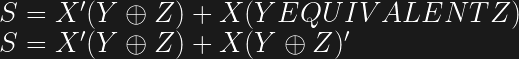
Let’s simplify the expression by substituting K for (Y ⊕ Z) to make the next step more clear.

This simplified form lets us see that again we have an XOR. We refactor to use the XOR operator and replace K with its original value.
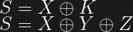
This is the final expression for the sum which is known to be true because any XOR of multiple inputs is 1 when there are an odd number of inputs. There is however some controversy over this interpretation of multiple input XOR.
Returning to the carry expression, repeated here, we reorder the expression and factor out Z in the first two sub-expressions. Here again there is an XOR operation so we do that refactoring.
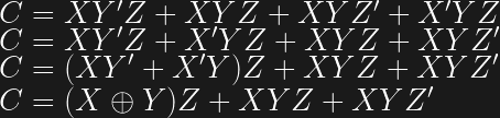
Now factor out XY from the last two expressions. From the identities listed above we know the sub-expression (Z + Z’) is always 1 so can be eliminated. That completes the math for the carry expression. The sum expression is repeated we can examine both final expressions.
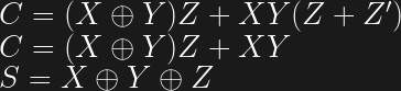
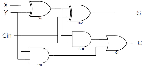
Obviously we can use the expression (X ⊕ Y) for both calculations in the logic diagram. Now we have the final full adder circuit design.
As nice as this design appears, it is not practical as an accumulator, e.g. a register for adding many bits at one time. If you want to add a 32-bit number you need one of these circuits for each bit. The carry input to a circuit comes from the next lower bit. Once X and Y for all 32 bits are asserted, the carry from the least significant bit is propagated to the next higher bit. In turn that carry propagates upward and this is repeated until all 32 circuits become stable. The propagation through the 32 circuits takes a comparatively long time. A modern multi-bit parallel accumulator is designed from the beginning as one circuit to attain high speed operation.
A design like this was useful at one time, and might be today in a system with space and power constraints. Some early computers performed operations, like addition, on serial streams of data instead of the parallel operations of today. Two shift registers, each containing one of the X or Y input values, would be shifted through this adder with the carry being held for the next shift period. The sum result would be shifted into another register, or perhaps the X register, to store the result.
Wrap Up
Switching or Boolean algebra is not restricted to hardware design. Modern software languages provide boolean variables and these techniques are equally applicable. Of course compilers will do some refactoring to optimize boolean expressions but the amount of improvement is uncertain. If a complex logical decision is needed it might be useful to apply these techniques.
An important resource I used in preparation is the WolframAlpha site which allowed me to validate the math expressions. Given an expression, the site generates the truth table, multiple refactorings using different operators, a diagram, and other information about the input. The truth table allowed me to verify my starting and factored expressions generated the desired output.
Another link to information about switching algebra that you might find interesting is Applications of Boolean Algebra: Claude Shannon and Circuit Design: a summary of switching algebra. I also referenced the site All About Circuits, Chapter 7: Introduction to Boolean Algebra throughout the article to provide background for a topic. The entire site is a useful reference for the electronics hacker.
This is the fourth article related to Shannon I’ve written. The first two articles touched on a paper he published in 1948 that created the field of Information Theory. The first discussed his analysis of the quantity of information that can be passed error free through a communications channel. This work lead to research on how to achieve maximum throughput using error correction techniques, the topic of my second article. Shannon’s Centennial Birthday celebration was on April 30th, and it also received an article.
This finishes the tour of Shannon for me, but not of all his works, or all the work others did based on his brilliance. There are any number of articles that can be written on information theory and communications and I may be back with some of them.


In your first conjunction/disjunction equation the symbols are switched. The dot should be with AND and the + with the OR.
Fixed. You’re right, the symbols were wrong.
The statement about when which one is true is switched around. It should be Disjunction: =1 unless x=y=0 in which case =0, and Conjunction: =0 unless x=y=1 in which case =1
There’s an enjoyable online class through Coursera that covers this and much more called VLSI CAD: Logic to Layout. Shoutout to Rob A. Rutenbar and University of Illinois at Urbana-Champaign for prodiving this course. I enrolled late just as a curiosity but I’ll be taking it again hopefully for a certificate.
What was the point of drawing out the karnaugh map of you weren’t going to use it?
the point of the km is to aid simplifying
take the carry table, there are two groups, the three 1’s in the bottom row and the two 1’s in the third column, you can say for the first group already (x and (y or z)) because its in the x row its x and, because it covers y or z its x and y or z, the second group you can say y and z (we cover x 1 and 0 so it is ignored). so then you can or your groups (expressions) == (x and (y or z)) or (x and y)
the mathematical (dull) method of refactoring can be done without the map just by using the truth table.
the groups thing works because of the gray code used rather than ‘normal’ binary, that is literally what karnaugh maps were invented for. you guys are fucking with me right?
Yeap, they are fu*king with you.
They used the truth table to make a standard sum of product form. It is easily proven that each “1” in the K-map is one standard product and that the poster should have done the graphical minimization of C instead of mathematical refactoring (unfortunately sum can’t be done easier if the reader doesn’t recognize the XOR directly from the K-map).
I’m rather disappointed that the full adder wasn’t made out of two half adders and one “AND”. Reusing smaller modules is a much better and easier way to do stuff.
Source: I teach Digital circuits at a local polytechnic.
Math and numbers leave me cold, but this subject leaves me at absolute Zero. I see both states at the same time as I can’t think at one bit level.
That has the stench of troll about it, but I’ll share this with you anyway.
You can learn to simultaneously visualise all of the possible logic operations with 2 inputs and 1 output by their combination with 4 gate type selector ports.
It looks something like this:
http://i.imgur.com/AAWkVWW.png
Can you think of another way of showing it?
Odd, image may be corrupted.
here it is again.
http://i.imgur.com/dfSPuO4.png
The heck with Karnaugh Maps. You all need something to waste more time on. https://en.wikipedia.org/wiki/Laws_of_Form
Why in blue blazes did the people who devised this, choose to re-use previously defined math symbols. I understood the logic just fine, but constantly having to translate it just sucked. My brain is already trained to automatically recognize those symbols. …Now remember people, purple means left now, and black means go. !Liking it.
When did we stop calling it Boolean Algebra? And when did we stop using !A to mean NOT A and switched to using A’?
Boolean algebra is applicable more generally than for switching circuit design. Shannon called it switching algebra so I followed his usage.
The use of the apostrophe is the classic usage for circuit design as presented by Shannon in his original work. The exclamation is for programming languages. There is also the convention in circuit analysis of a horizontal line above the variable or expression.
Don’t forget the tilde, encountered those in the suite we used to program GAL, PAL, CPLDs
You might want to re-submit this with modern symbology, with just a passing reference to the original method. Unless this was just meant as a history lesson.
What is the modern symbology? I assume this course material is modern and if follows the symbology I used: https://cseweb.ucsd.edu/classes/sp08/cse140/lectures/wk1d2.pdf
We each encounter material like this from different source materials. They simply do not agree on the representation of negation. You’ll find the apostrophe (‘), the trailing exclamation (A!), the leading exclamation (!A), the leading tilde (~A), the top bar, the dash with a tail (¬A), and even just a minus sign (-A).
There is nothing stopping you from producing a version that suits you and then submitting it yourself. The quickest way to do this is to use your favorite editor and convert the page to .PNG format, via PDF if required. You can then upload that image of the page to a free imaging host and add the URL to your comments so that everyone can see the page. Otherwise there is always the more formal HAD editorial route, either way there is no excuse for just sniping and criticizing in a manner that is not constructive or useful. . .. . … .. .. .. . … . … . .. …. . .. .