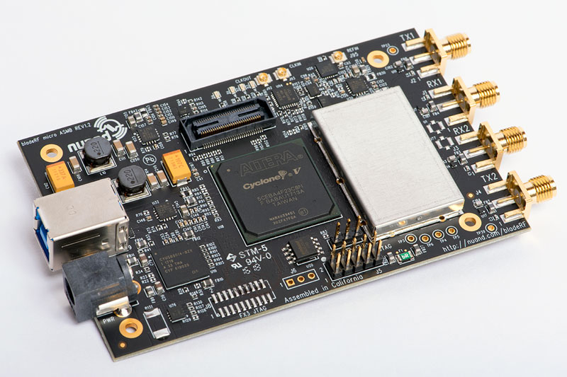
When it was launched in 2013, the BladeRF was one of the most powerful of the new generation of Software Defined Radios. Now, Nuand, the producers of the BladeRF are looking to up the ante again with the BladeRF 2.0 Micro. This new version has a huge list of changes and improvements, including a more bad-ass FPGA processor and support for receiving and transmitting from 47 MHz all the way up to 6 GHz, with 2x MIMO support and an impressive 56 Mhz of bandwidth. It also retains backwards compatibility with the original BladeRF, meaning that any software written to support it (which most SDR packages do) will just work with the new device.
At the heart of the BladeRF 2.0 Micro is an Altera Cyclone V FPGA. Nuand are producing two versions of the Micro: the $480 xA4 uses the 49KLE Cyclone V FPGA, while the $720 XA9 is built around the 301KLE Cyclone V FPGA. The extra power of the xA9 lies in the larger amount of logic gates and elements on the FPGA, which means that the card can do more signal processing itself. That should make it easier to create stand-alone devices that process a signal and output the results. Nuand demonstrated this on the BladeRF by creating an ADS-B receiver that ran on the card itself, outputting the decoded airplane data to the USB port. The xA9 could do significantly more than this, and the possibilities are intriguing.
The new card is also, as the name suggests, smaller, measuring 2.5 by 4 inches, which would make it easier to integrate with devices like the Raspberry Pi, although it is still a little larger than the Pi.
The SDR marketplaces has changed a lot since 2013, with a profusion of cheap, open-source SDR receivers and transceivers like the LimeSDR and SDRPlay. These devices are cheaper than the BladeRF, and offer most of the same features. So, is there still a place in the market for a more powerful, more expensive device like the BladeRF 2.0 Micro? That, as they say, is up in the air.


The most strategic change is that they have upgraded the LMS6002M to a AD9361 as their transceiver chip (the same chip that is used by Ettus Research in their B210). Basically they have stopped giving money to Lime Microsystems, who are now a direct competitor. And they are now giving money Analog Devices who are not a direct competitor because they are in a slightly different segment of the SDR market with their USB 2.0 PlutoSDR device.
Sorry LMS6002D (not M)
A refresh in Lime’s line would be LMS7, but with 10 bit ADC it is rather low-end chip, just a notch or two higher than HackRF or RTL. Nuand has no chance to compete with a company controlling entire food chain, so I’m glad to see that they opted for a more expensive, but significantly better solution.
The LMS7002M is 12-bit as well ( https://wiki.myriadrf.org/LimeMicro:LMS7002M_Datasheet#Features_summary )
12 marketing-bits. ENOB is 9 bits. Even worse than what I wrote. Check tables 16 and 17.
I totally agree, but the LMS7002M can also sample at 160 MSPS and decimate inside the LMS7002M, so it can get an extra half a bit from that. And the ENOB (or SNR) for the AD9361 is not given in the datasheet on anywhere on the analog website that I can find which probably means that it is in and around the same.
Don’t get me wrong I do know that the AD9361 is a better chip than the LMS7002M, but both have oddities that are not obvious from the reading the datasheets.
According to Analog Devices, the ADC sampling on the AD9361 (and consequently the bladeRF 2) is 640MSPS, https://wiki.analog.com/resources/eval/user-guides/ad-fmcomms2-ebz/ad9361
@bluescript Very interesting so they would get about ~1.66 bits of extra dynamic range from the ADC at 64.11MSPS by oversampling at 640MSPS and decimating by 9.98.
But without knowing what the baseline ENOB (or SNR) is, it does not provide any meaningful information.
But if they are sampling at 640MSPS and fully compiling with ITAR/EAR CATEGORY 3 devices:
Then the ADC would fall under under section a.5.a.1. “A resolution of 8 bit or more, but less than 10 bit, with an output rate greater than 1 billion words per second;”
And not under section “a.5.a.2. A resolution of 10 bit or more, but less than 12 bit, with an output rate greater than 500 million words per second” So the actual ADC must be less than 10-bits.
So that would mean that it is probably a 9-bit ADC that is oversampling.
No sorry I misread that, it is either 10-bits or 11-bits and would directly fall under a.5.a.2.
And it would not under a.5.a.3. A resolution of 12 bit or more, but less than 14 bit, with an output rate greater than 200 million words per second;”
So it is is a 10 bit or 11 bit device that is oversampling.
ITAR/EAR have changed the phrasing over the years (as well as upping the sample rates) it was not “output rate” in the past but since they specify that and IF there is no way to access the samples at 640 MSPS, then it would be legal to publicly sell end user devices without the usual signed in triplicate with human blood ITAR requirements.
$720 you’re going to feel that. Still wondering when cellular chips are going to swayed into the SDR side?
LMS6/7 are cellular solutions.
Transceiver:
https://upload.wikimedia.org/wikipedia/commons/thumb/2/22/SDR_et_WF.svg/500px-SDR_et_WF.svg.png
And yes it’s an improvement.
Yea $720 is huge bite, out of a hobby budget, and that doesn’t include a computer. However when care is taken to compare apples to apples is it really that much more expensive than the 6M and up multi mode transceivers that used to be offered by the ham radio big three? Any thing that goes beyond 70 cm, that the now ubiquitous MF/HF/VHF/UHF rigs, that often require optional equipment to cover some bands. I’ll never live long enough to be able to play in that playground, not something I will sweat.
^this, you will be hard pressed to find a quality 2 meter/440/6 meter rig with digital features under a thousand dollars these days.
for something that covers orders of magnitude more bandspace, totally worth the price.
The $720 xA9 is the larger FPGA (300KLE is a lot!) variant which seems to be a better fit for doing a lot in the FPGA. That being said, it’s likely the cheaper xA4 is good enough for purely software applications.
Thanks for the information.
I scanned the product page without seeing the obvious specs. How many MHz can you watch/listen to on a waterfall at once? Could I monitor the entire 144Mhz to 148Mhz of the 2M ham band at once? How is the max transmission power?
Yes the whole band.
CW +8dBm
https://www.nuand.com/bladerf-2-0-micro/#blade-featured-wapper
The maximum TX power would be, at a guess, by default the same as any other SDR with TX that is sold as a FCC 15.103 exempted device under section C “A digital device used exclusively as industrial, commercial, or medical test equipment.” (somewhere in and around +10 dBm give or take a bit appears to be what is used for commercial test equipment). I’m sure that is documented somewhere but I can’t find the FCC document that specifies what is acceptable for test equipment.
It would be useful to know how many applications ever exceeded the capability of the little-FPGA version of the last one. I don’t have a sense of whether the upgrade is actually likely to be useful, or is an academic point that you’d need to go out of your way to take advantage of.
Depends what you plan to do. If you’re interested in implementation of algorithms in hardware, bigger fpga will give you more room to play. If all you’re going to do is to use the board as an RF interface to the computer, the small fpga should be perfectly fine.
What would it take to use this as an emissions testing device for EMC purposes? Attach a wireless antenna for radiated power, and some kind of attachment to strap to a PCB trace to measure the spectrum of DC/DC converter?
I suppose calibration would be difficult.
You could use a TEM cell as replacement for an anechoic chamber. This also allows you to do immunity testing with little input power. You can build one yourself. Calibration is difficult but to get an indication before going to the lab it is perfect.
calibration would most likely be just expensive :P
My guess is you would be better off with buying a precompliance EMI reciever that is actually built for this kind of work. It does not take an R&S ESW monster to get a good idea about your device. But having the right quasi-peak and CISPR-RMS detectors, a low frequency input (down to 9kHz), so you can measure conducted emissions too, and not just radiated emissions above 30MHz is actually worth it. If it’s more of a “one time only” thing, you better go to a EMC lab for a day or two. They not only have the equipment and know how to use it, but can at the same time give you valuable advice on what to tune, if your device does not pass.
Sorry for being a bit of a grammar nazi, correct me if I’m wrong, but shouldn’t markets be plural in
“The SDR marketplaces has changed a lot since 2013”?
no
I’m surprised it isn’t using the Cyclone V SE. Being able to mix conventional 32 bit CPU cores with accelerated blocks on the FPGA fabric should cut down the complexity a fair chunk.
One thing that slipped past me is printed at the bottom of the PCB “assembled in California”!
An AD-FMCOMMS3-EBZ is about the same price, about $700 or so IIRC.
Sure, you need to add the Zedboard or other board with a FMC port, so there’s another $400 or so.
But you don’t need a PC – just add monitor, keyboard and mouse, and the ARM9 IP core on the Zync gives you everything all in one place as a self-contained solution. And you’ve got LEDs, switches, PMOD ports etc, an FMC port, ethernet, audio etc – everything you need for other FPGA development projects. Nice and flexible and not that much more expensive, all things considered, compared to these single-purpose AD9361 boards.