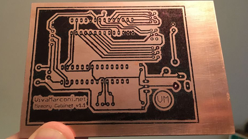
Right now, you can design a PCB, send it off to a PCB fab, and get professional finished boards in a few days for less than a dollar per square inch. This is fantastic, and it’s the driving force behind ever-dropping costs of hardware development. That’s great and all, but you can make circuit boards at home, easily, and without involving too many toxic chemicals. That’s exactly what [videoschmideo] did, and the results are pretty good.
The process starts with a single-sided copper clad board that would be readily obtainable at Radio Shack if there were any of those around anymore. Once the circuit is designed, the traces and pads are printed (mirrored) out onto sticker backing paper. The toner from your laser printer is transferred to the copper with a clothes iron.
The tricky part about creating a PCB is taking away all the copper you don’t want, and for this tutorial [videoschmideo] is using a vinegar and hydrogen peroxide process. If you’re using stuff you can buy at the grocery store, you’re only getting 3% acetic acid and 3% peroxide, but given enough time and enough peroxide, it’ll do the job. After the board is etched, [videoschmideo] neutralizes the copper acetate produced with aluminum foil. The end product isn’t the safest thing in the world, but aluminum salts are much more environmentally friendly than copper compounds.
Making PCBs at home isn’t anything new, but it’s nice to be reminded that you can do so even with minimal effort and chemicals that you could rinse your mouth with. Once you do, though, you’ll probably have to drill some holes in the board. Yes, you could use a dremel, but a nice small drill press is a pleasure, and well worth the investment.


I have recently discovered that the toner ink can be transferred chemically, with “nail polish solvent” and basic glossy paper… but I have become lazy these last years so I doubt I’ll try.
That sounds interesting. Can you give more info?
Perhaps Yann means this?
https://www.youtube.com/watch?v=cVhSCEPINpM
It’s been on HaD before. Search and I’m sure you will find a step-by-step.
Nail polish remover is usually acetone, mixed with water, and with “nail nourishment compounds” added, perhaps to compensate for the nastiness of acetone. I might worry a bit about the various traces of “nourishment” or “protection” or whatever in the process.
If it works then presumably acetone will work, probably better.
As far I know most nail polish removers stooped using acetone as main ingredient
CVS sells nail polish remover consisting of 100% acetone under the Beauty360 brand. A big red “Pro Strength” is on the label.
It turns out that it’s cheaper to buy this nail polish remover acetone than actual acetone from the hardware store.
I tried this last time Mike posted this in 2012 but with toner transfer onto photo paper, tho printing to sticker backing paper is new to me. It worked alright, a bit slow tho.
https://hackaday.com/2012/02/15/etching-pcbs-with-vinegar/
I have problems with holes in the toner coverage on sticker-backing paper as it comes out of the printer, but it peels off great. For thick lines, it’s probably not a problem, but I always have a good look befire etching.
Better than either photo or sticker paper, IMO, is thin glossy newsprint like you get in magazines or some catalogs. Toner sticks better to it in the printer, but most of the paper just dissolves off in water with gentle rubbing. If some sticks to big ground-plane patches, so be it — don’t abrade the toner trying to get it off.
I’ve used the New Yorker and the Economist with equal success, despite the fact that one’s a bit leftish and the other laissez-faire-to-right.
Ferric chloride is pretty safe, just don’t get it on your clothes or carpet.After a bit of practive I managed to reliably make double sided PCBs for things like STM32 in LQFP-100 package. Getting registration of images right takes a bit of practice but can be done.
PROTIP #1: Your print might not be 100% dimmensionaly accurate. Doesn’t really matter for DIPs or THT compnents, will be a PITA for SMDs. While printing my PCBs I had to scale them horizontally to 101,2% normal size.
PROTIP #2: Don’t waste your time and money on cheap “HSS” drills. Not only they vibrate at high RPMs, they’ll get blunt in no time and will likely mess up your precious PCB. Get a PROXXON mini drill (FBS240 is fine) with a stand. Buy proper PCB drilling bits and run them at 20k RPM – they look like these https://1.allegroimg.com/s512/01f9fa/7bd4b5c94165b03e18b1ac166641 This way you’ll repeatedly make nice 0.3 or 0.5mm holes without messed board. Just be careful, they’ll break easily if your PCB moves while on the drill.
Some ex-employee at management level decided to revenge dump a load of spares leaving on our company logo as a setup… fortunately for the company the ex-employee fly-tipped it onto some land owned by my brother’s friend so I was able to explain the situation and offer clean-up help, I was granted to help him out and thus got to rummage through the dumped stuff.
Amongst the random spares were a load of these drill bits as per your link, just RScomponents branded.
I had recovered a load of those drill bits of varying sizes along side some interesting DIP packages. Of course, now I only have the larger bits left as I snapped all the useful size ones due to using them how they wern’t intended as I’d use them by hand a lot at work for drilling out the solder mask paints from vias to solder in repair wires though they lasted a surprisingly long time under my abuse.
>without involving too many toxic chemicals.
Don’t believe the ”toxic” BS that they spread. Do you own research.
Avoid the vinegar and salt mix (not used here) as it produce chlorine which is toxic. Just because they use 2 safe kitchen item doesn’t mean it is safe because chemical reactions.
Ferric chloride is actual safe. Source: https://en.wikipedia.org/wiki/Iron(III)_chloride#Industrial
>Iron(III) chloride is used in sewage treatment and drinking water production
HSS are less likely to break when you don’t have a proper drill stand.
I used Copper Sulfate (CuSO4). Was available at garden store. With right proportion and temperature of water and salt the etching time reduced to 8 minutes. The trick is to use right proportion.
I’m not sure if it’s typo in the article, but baking paper is pretty good for toner transfer method. It’s heat resistant and glossy but toner will stick to it and easily transfer to board when heated with clothing iron. One additional trick after transfering toner to board is to heat it with hair dryer (or paint removal hot air blower, or hot air rework station) so toner will melt a bit and fill miniature holes that transfer left. After a bit of practice you can make toner transfer method pretty reliable. Even though I always liked photo method better, once you get right timing it works every time without need for fixing.
I did toner transfer PCB etching, but I stopped, because I had huge problems with “toner opacity” – I wasted too many boards because sodium persulfate got under the toner. I tried both reheating the toner on PCB to melt it, acetone vapor process and even leaving paper on the toner, and combinations of these techniques, but it didn’t help much. I switched to photolithography, but that has its own problems, including getting PCB uniformly coated with photoresist, exposure times (under- and overexposure) and getting unexposed phooresist to stay on the board after exposure. I switched to PCB factory but that’s just too expensive. I’ll try CNC next…
I tried hybrid process on 3d printer. Works pretty well (could be better though) – https://hackaday.io/project/160688-turning-3d-printer-into-engraver .
I tried several printers.
Brother printers don’t well because they use a low temperature toner.
I get good results with HPs and Xerox.
I moved on and made a toner transfer fuser from a laminator and started using Pulsar Toner Transfer Paper and the green foil and I very very good results from that –
https://cdn.hackaday.io/images/9345931458294540615.png
The distortions at top left and bottom right are bent pins.
I just realized that this pic is a bought breakout but the quality is the same.
Except for the solder mask of course.
Another example –
https://cdn.hackaday.io/images/4747701466897513322.jpg
Can you reveal to us what that is?
“Top Layer”
Hm. I made a Top Layer once, but it didn’t look anything like this.
i’m betting on a fpga scsi to ata converter, plus jtag
I hae a LG ML-1710…
Totally second the endorsement of HP printers — had bad luck with a Brother and a Samsung, then I picked up a used laserjet 2300 on ebay for like $25. Cheaper than the toner.
And make sure that you get 1200 DPI resolution. If you get your transfer skills down, you’ll see the dots from 600 DPI.
I still like CNC PCBs even though I use 20 mils clearance in my designs to compensate. It’s very sensitive to depth of cut and I sometimes get high impedance bridges where I don’t want them (I think from flux). My latest trick is to rub some “polishing compound” over the PCB after isolation and then have the CNC go over it with a wire brush tool to remove the burrs. I pre-drill with the isolation tool to half depth just to guide the drill bits later on, which otherwise wander. And yes, I use OSH Park and Seeed (white solder mask) too. Home-made PCBs is a hobby for me. And I’m impatient.
I mounted a 2.5W laser on my 3d printer, painted PCB with regular black paint from a can. Then I burned the paint away with the laser and get this result:
https://imgur.com/a/02VezXj
It takes some time to burn the paint but no more fiddling around with paper and iron! Much easier and consistent.
On the software side I used Eagle, exported the PCB into dxf file and then imported into Visicut http://visicut.org/
That just may be sufficient incentive to go ahead and buy a laser for my CNC engraver. Seems a LOT less fussy than toner transfer.
That’s impressively clean. I tried ablating paint with a laser cutter a while ago, but never got it to work without a bunch of the paint (or gunk created by burning paint) re-depositing on the newly cleared copper. Did you have to fiddle around to avoid that sort of thing, or did this just work?
It just worked fine, I only used a hard kitchen sponge to remove the burned paint residue. Few rubs and it all went away fine.
You can get 30% peroxide in a pharmacy or a hunters store, they use it for bleaching deer skulls. It really accelerates the process
I don’t understand why presensitized boards don’t get more love? Sure they cost a few bucks more, but if you’re really trying to save money why are you DIYing it anyway? OSHPark and done.
…perhaps i can have PCB in 60-90 minutes done at home…
for some countries OSHpark is delivery time really long vs. homemade pcb
I can etch a presensitized board in about 60-90 minutes, too. The common complaint is it is more expensive, but if you’re really trying to save money you won’t DIY as all methods are typically more expensive than say OSHPark. Not just raw materials costs but also your labor.
If you can’t find any? In your locality?
I can’t find any in my locality, either. Got mine from Amazon but there’s also Jameco, Digikey, Mouser, eBay, Ali, BangGood…
Presensitized boards work too. It’s one more chemical step and getting the tradeoff between exposure time and toner thickness (on the transparencies) is a bit trial-and-error, but once you’ve dialed it in, it’s easier to get consistent results than with toner transfer, IME.
You can also, in principle, get finer features with photo boards, but it’s in the same ballpark as toner transfer, so this isn’t a big difference. You’re reliant on the laser printer in the end either way.
For price, you can also get photofilm and stick it on yourself, which might be cheaper than boards with the film already on them, but is still a bit more expensive than toner transfer onto blank copper.
I’ve become too good at toner transfer to do anything else (here’s how) but if I had something to directly expose the boards, skipping the laser-printer-on-transparency step, I would switch to photoresist.
https://hackaday.com/2017/06/15/laser-pcbs-with-ldgraphy/
https://hackaday.com/2012/08/09/exposing-pcbs-with-a-home-made-laser-printer/
https://hackaday.com/2016/03/03/etching-pcbs-with-a-3d-printer-2/
https://hackaday.com/2017/07/14/laser-exposing-pcbs-with-a-blu-ray-laser/
etc…
This guy uses mineral oil on paper to create a transparency. The oil makes the paper clear enough for sunlight UV to pass through. I’ve not tried it but he shows it being done with ~60 seconds of sunlight exposure. Pretty neat.
https://www.youtube.com/watch?v=b16SI1V7u0w
I use the pre-sensitized boards. Simple, and repeatable. No ironing required.
I make resist masks for home etched PCBs out of adhesive vinyl on my Silhouette paper cutter. The end result is really clean looking and there’s no schmutzy black toner stains left behind.
My dollar store bottle of vinegar says 5% acetic acid by volume.
Here we go again!
It seems like every few years HaD goes through a round of people claiming to have etched boards using vinegar and hydrogen peroxide. I tried by following the directions in past HaD articles. All I ever got was a grayish coating of some sort of corrosion over top of a very much extant layer of copper. I even tried keeping a small piece of unetched PCB in jar of vinegar and peroxide for a couple of weeks. It didn’t seem to have any effect at all!
Is this some kind of joke or what?
I believe it is a viable technique.
I use the homemade cuperic chloride method. It took me a while to get it to work well — at first I would just get a dull oxide layer and the etching wouldn’t happen unless it was in the tank for a hour or more. Over time I was able to refine my process and now I get a great board in just a few minutes. I suspect your efforts with vinegar and peroxide have some small details that makes it work well that need time and testing to get the hang of.