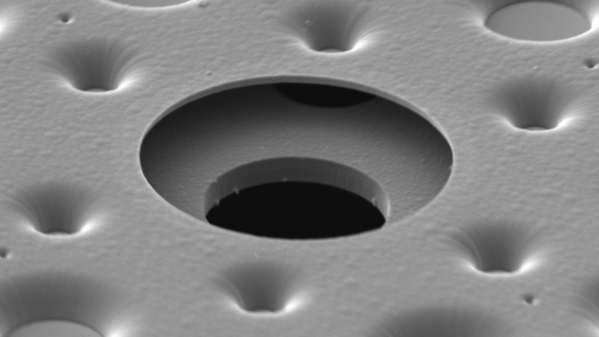
Now before you start asking yourself “best for what purpose?”, just have a look at the quality of the DIY PCB in the image above. [ForOurGood] is getting higher resolution on the silkscreen than we’ve seen in production boards. Heck, he’s got silkscreen and soldermask at all on a DIY board, so it’s definitely better than what we’re producing at home.
The cost here is mostly time and complexity. This video demonstrating the method is almost three hours long, so you’re absolutely going to want to skip around, and we’ve got some relevant timestamps for you. The main tools required are a cheap 3018-style CNC mill with both a drill and a diode laser head, and a number of UV curing resins, a heat plate, and some etchant.
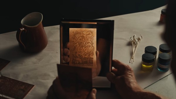
[ForOurGood] first cleans and covers the entire board with soldermask. A clever recurring theme here is the use of silkscreens and a squeegee to spread the layer uniformly. After that, a laser removes the mask and he etches the board. He then applies another layer of UV soldermask and a UV-curing silkscreen ink. This is baked, selectively exposed with the laser head again, and then he cleans the unexposed bits off.
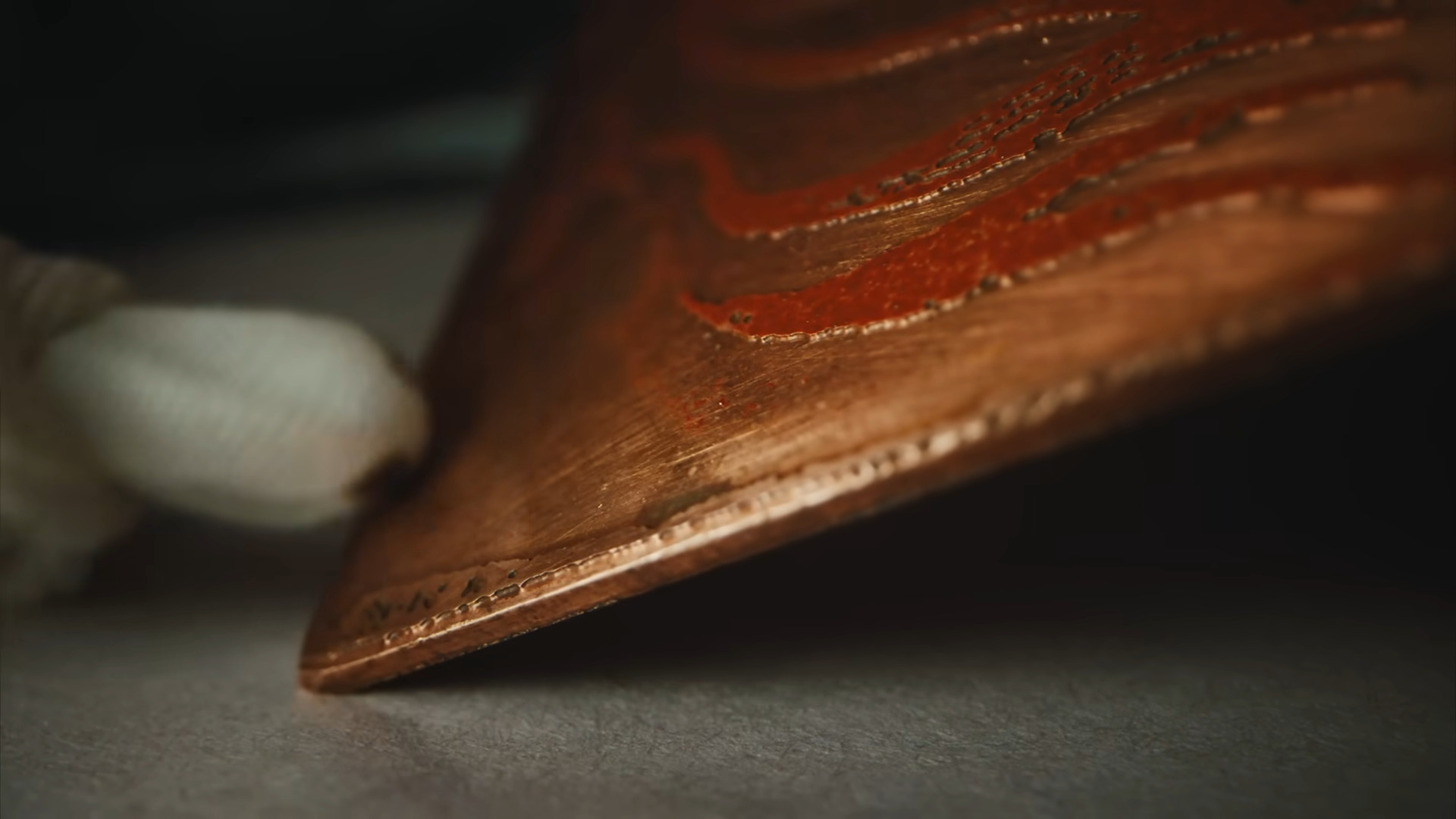
In the last steps, the laser clears out the copper of the second soldermask layer, and the holes are drilled. An alignment jig makes sure that the drill holes go in exactly the right place when swapping between laser and drill toolheads – it’s been all laser up to now. He does a final swap back to the laser to etch additional informational layers on the back of the board, and creates a solder stencil to boot.
This is hands-down the most complete DIY PCB manufacturing process we’ve seen, and the results speak for themselves. We would cut about half of the corners here ourselves. Heck, if you do single-sided SMT boards, you could probably get away with just the first soldermask, laser clearing, and etching step, which would remove most of the heavy registration requirements and about 2/3 of the time. But if it really needs to look more professional than the professionals, this video demonstrates how you can get there in your own home, on a surprisingly reasonable budget.
This puts even our best toner transfer attempts to shame. We’re ordering UV cure soldermask right now.
Continue reading “The Best DIY PCB Method?” →