The lingua franca of electronic design is the schematic. I can pick up a datasheet written in Chinese (a language I do not read or speak) and usually get a half-decent idea of what the part is all about from the drawings. Unfortunately, even as my design experience has grown over the years, I haven’t quite learned to think in schematics — I need to see it on paper (or on a screen) to analyze a circuit. Whether it’s literally on the back of an envelope or sketched in the condensation on the shower stall, actually drawing a design or idea makes a huge difference in being able to understand it. And, if you’ve ever tried to explain a circuit without a schematic — in an on-line forum or over the phone, for instance — you know how difficult it is.
So, given the importance of the schematic for design and communication, you’d think choosing a tool to draw them would be an easy task. Not so. There are dozens of choices, from dedicated schematic drawing programs to using the schematic-capture facilities of simulation or PCB design tools, or even old-fashioned pencil-and-paper and its modern equivalents. Each one has its pros and cons, and may be better suited to one specific application, but you have to choose something.
So, readers of Hackaday, what do you use to convey your electronic design ideas to the world?
Old-school: Drafting
The simplest approach is just to take up pen and paper and get to it. The field of electronics obviously pre-dates modern computer UI’s, so there is a rich history of hand-drawn schematics; just open any book from before the integrated circuit era to see some. This approach offers the ultimate flexibility – you can generally use anything at hand to draw your circuit, from your antique oak drafting table and Rapidograph pens to a stick in the sand. The downside is that if you’re not an artist (or skilled drafting technician), your schematics will certainly reflect this, as mine do. But, it’s easy, quick, and portable.
The next step up is virtual pen-and-paper: a general-purpose drawing program. Although I admit to drawing a few schematics in Paintbrush under Windows several decades ago, your best bet is probably a vector drawing program. I know it shows my *nix graybeardedness, but my go-to drawing program is xfig. There are many more modern alternatives, including Dia and Inkscape, while readers can certainly recommend tools specific to other platforms. A convenient way to use a package like this is to build up a library of symbols that you commonly use. This gives you flexibility to draw them as you like: you’re free to draw your resistors as little boxes, while I’ll keep my squiggles. The downside is that you’re basically starting from scratch, although some packages may have electronics symbol libraries you can leverage (xfig does, but I don’t like their look).
One disadvantage of either approach is that you can’t generate netlists to import into simulation or PCB layout tools, but if you’re not going to use either one, this doesn’t matter.
Dedicated Schematic Capture Programs
Stepping up from general-purpose drawing tools, we come to packages dedicated to schematic drawing. The first one of these I ever encountered was XCircuit, another relic from the good old UNIX days. The stated goal of this program is to produce quality output for publication, as opposed to schematic capture for further processing. A little searching also turns up TinyCAD, which does output netlists, but also claims high-quality output suitable for publication. Learning one of these tools never quite seemed worth the investment, since they are targeted at such a specific niche purpose. Every other tool category I’ve considered has a secondary use — for example, time spent learning Inkscape to draw schematics could be leveraged to use the program for any number of purposes. Maybe these tools are perfect for my use case, but I just haven’t given them a shot?
Simulators
Modern circuit simulators come with relatively decent user interfaces, although each has its quirks. Conventional wisdom is that like PCB layout programs, you carefully choose one that best suits your needs, then complain loudly about it. Of the several simulation tools I’ve used, I’ve logged by far the most hours using LTspice, the free (gratis, not libre) simulation tool from Linear Technologies (now part of Analog Devices). If you need to simulate your circuit anyway, you can sometimes kill two birds with one stone by using the schematic from your simulator for publication. Of course, for simulation purposes, you may include some parts (parasitic components, for example), that won’t be listed in the BOM, and substitute voltage or current sources for whole subsections of the design. These changes cause the simulation schematic to diverge from the published one, so you may end up drawing it twice anyway.
One advantage I’ve found to this approach is that all the components have presumably been drawn to be “compatible” — in the same style and scale.
PCB Layout Editors
CAD programs for PCB design also feature schematic capture facilities you can leverage to generate diagrams for publication. I happen to use Eagle, although I know there are a lot of KiCAD types out there. Either one, or any number of alternatives, would provide the same functionality. There is typically a closer match between the schematics captured for PCB layout and publication than those used for simulation, although sometimes it’s useful to show more information than you need to design a PCB — a simplified diagram of the internals of an IC, for example. The biggest disadvantage I have found is that symbols from different libraries may be drawn in a different style or at a different scale, making for an ugly schematic output. As a result, I’ve ended up re-creating my own library of symbols, which also eliminates any licensing concerns (I care more about the license of designs I create than of the tools I’m using).
To Cloud or Not to Cloud?
All the tools I’ve mentioned above are traditional desktop applications, which I prefer. Of course, there are now cloud-based tools in each of the categories. I haven’t explored this space very well, although I’m certainly aware of circuitlab, which is the preferred tool for schematics on Electronics.StackExchange, and the Falstad circuit simulator, which sees occasional use on hackaday.io. I’m sure there are other tools out there, but my reluctance to adopt a cloud-based workflow has kept me from fully investigating the options. Maybe I’ve missed exactly what I’m looking for?
Your Turn
OK, Hackaday, what tools do you use to produce schematics? Are there tricks that make one particular tool easier to use for this purpose? Does everyone end up with a mishmash of tools like I have, or have people figured out how to get all the functionality they need from just one? Let us know in the comments below.


Straight to KiCad. Especially since 5.0/5.1, it’s a breeze.
Preach it.
Just did a porting project with kicad, and the libs from digi-key made it actually a time saver.
Very nice long-term documentation option… once you learn the nested-sheet concept.
“To Cloud or Not to Cloud?”
https://en.wikipedia.org/wiki/Betteridge%27s_law_of_headlines
;-)
KiCad
KiCad has non-standard symbols, incomplete default symbol library, and extremely annoying part labeling: it tries to make all parts a rectangle, and write the value inside the rectangle, even vertically, which is hard to read and the just wrong thing to do.
I was able to get it to do something ‘normal’ (everything should be readable, and without rotating the schematic 90 degrees), but had to override every component I placed.
I agree, I am a bit underwhelmed with KiCAD too also. I think it’s a great idea, has a lot of interesting features but is difficult / clumsy to use. My favorite over the years was ProCAD, which has long since bit the dust. I like Altium’s CircuitMaker, which I understand has ProCAD as part of its ancestry. That’s probably the one I use the most these days. I also like DipTrace. I have used Eagle from time-to-time and it works okay, my only “complaints” about Eagle and DipTrace is that they don’t fit the “intuitive feel” I’ve become accustomed too from Microsoft Windows use– and I would LOVE to drop-kick Windows into oblivion if I could and just use Linux all the time, except the majority of the software that I use / like isn’t available on Linux, :-(
Sorry, I meant Protel, not ProCAD,
KiCad allows placing refdes and values anywhere you like. It can be frustrating at first, but after a bit of initial hardship the payback is good.
I find that KiCad was built with a specific workflow in mind. When you learn that workflow, everything fits together really well. It does have a learning curve to figure out how make all the pieces work together, though.
Custom library management is a mess, though.
I agree on both accounts. Specific workflow in mind is a great thing and it sets KiCad apart from some other tools. Library management has always been a terrible mess in KiCad and there seems to be nobody with a clear vision of how it really should be done. It’s a shame, because it seems that a lot of potential newcomers expect to find ready and easy to use libraries.
Thank you. Nice program, but lots of hype too.
Did you try placing a cursor over the part and pressing the “O” key? It tries to rotate the label to horisontal position and place it so it does not collide with anything.
KiCAD.
If I was just doing schematics for illustrations, DipTrace. It is the closest to Protel99, which I would still be using if I could afford the Altium updates.
Altium has a free / hobbyist edition which I use all the time. I agree with you about Protel. That’s the one I really liked.
And there’s also the Circuit Maker which is a stripped down AD but still useable.
How big is the learning curve going from Eagle to KiCad? How difficult is it to import custom libraries created in eagle? Losing my custom library is one of my main sticking points for making the jump.
Nobody will ever know. Once one system is learned, the user never switches. That’s why Eagle has a free version.
Many years ago I ditched Eagle for Kicad, because of the silly limitations in Eagle and it really wasn’t that hard to switch, so I wish I never spent time on Eagle in the first place.
How different is riding a mountainbike from riding a racing bike? It’s different. You can get around on both, but it has a different feel to it.
More like driving a ‘Murican automatic on the interstate vs. driving a manual Fiesta down an Irish lane, shifting with your left hand.
I recently converted and have found most things easier once you learn KiCAD. The biggest difference is how parts are handled so your concern is on target. Doing a Google search reveals much information on importing Eagle parts into KiCAD. I’d say that the time spent on the KICAD learning curve is worth it for me.
I have found the initial re-learning of how to do steps is quite difficult. But then, it is learning by doing. KiCAD has
different concepts compared to EAGLE. In KiCAD, I had to think a lot about ‘intent’ and design workflow. EAGLE is more focused on concurrent editing of schematic and layout while KiCAD is more of a ‘Make schematic & add values to symbols, annotate schematic symbols, Assign Footprints, import to layout editor’ rigid workflow. Once you get the workflow and ask yourself why it has been done this way, KiCAD is just as good as EAGLE.
In EAGLE, every part has a footprint assigned or some variants. Once you add a resistor, you already chose its associated footprint. In KiCAD, the philosophy is different: You can pick a resistor from the symbol library and add as many as you like. After placing none of them will have a footprint assigned. You now can assign footprints to each resistor (This can of course also be done in a central place for bulk assignment).
KiCAD also does not annotate for you. It keeps parts unannotated (eg L?, C?) until you annotate them. Coming from EAGLE, I was using the ‘Annotate’ button way too often. It makes sense, though: After placing, automatic assignment of names is not neccessary. It only becomes important when assigning footprints to symbols before the PCB routing. This can and should be done in bulk anyway.
In KiCAD, symbols and footprints are intended to be separate in different libraries. This allows for re-use of standard footprints like SO8 or QFP32. EAGLE requires a library to have the symbol as well as footprint. You can make do with copy and pasting for your own libraries for things like OpAmps and such but it is annoying to jump back and forth looking for the right footprint, etc.
EAGLE allows for netlist classes but does not depend on them as much as KiCAD does. Before going over to the schematic, assign classes like +5V, +VCC_DAC, .. to the relevant nets. This will make you find good names for your nets pretty quickly. You can then assign rules in the layout editor on width, spacing, vias for the different classes. You can of course do without them but it helps a lot in routing as it may with EAGLE (I have never used that particular feature in EAGLE at all :P ).
Those are the first thoughts which came to mind. Regarding the libraries: You may have to redraw your components, yes. Tech-debt can be annoying especially coming from a vendor lock. This will take time and was also the main reason it took me so long to switch to KiCAD. I tend to think about this differently now:
– The time I have spent recreating those components is neccessary for any switch to a different product.
– Using KiCAD, I can spend a little more time make pull requests to the KiCAD symbol/footprint repository.
– Both will be checked for correctness by librarians:
– I get someone checking my work for free.
– KiCAD profits by having another part in its library.
– I profit from having every part I converted directly in the upstream library.
– Everyone else profits from the 1-2 extra hours spent converting the part.
The process is a bit cumbersome and takes getting used to it. But after creating a few parts, one will find a suitable workflow, especially because most of it is git workflow. It also not always applies. For NDA projects, the parts will end up in a private library anyway. Then, nothing can be gained anyway :^)
A well thought out and detailed response. Thanks for sharing!
The learning curve is not difficult. The hard part is overcoming the constant frustration that things are done in a different way.
It took me a few tries. The Autodesk takeover did the final motivation for me. Now KiCAD feels as natural as Eagle once did.
It’s a decent tool. It sure is not intuitive, but there are tons of online videos to help.
You will be swearing a lot but it’s okay. Try a tutorial or two before committing to a full-sized project.
As for importing Eagle libraries, it should be possible but imho it’s faster and more rewarding to learn creating your own components in KiCad, you’ll need to add more of them anyway.
i really want a tool that produces a readable schematic from a text description of it. like openscad, but for schematics. where you don’t waste all your energy fighting some GUI. where you can get meaningful diffs out of your revision control system. i’ve embarked on this project a couple times but they were both false starts, i still haven’t got a grip on what the right level of abstraction is.
Because I write instruction-sheets for students, I usually have to draw nice-looking small diagrams.
For this I use circuitikz: the learning curve is hard, doesn’t scale well beyond 20 components in a single schematic, but it integrates nicely with LaTeX (it’s tikz after all). Have a look at this tutorial: https://www.latex-tutorial.com/tutorials/circuitikz/ .
hey thanks!! i’m not sure i like it, but it’s in the right family, and i can actually use it! tikz in general might be up my alley, really.
You can take a look at SKiDL (https://xesscorp.github.io/skidl/docs/_site/index.html). It’s a small package that lets you design circuits using Python. The output is a netlist that can be fed into PCBNEW to do layout. I know you want a schematic as output, but that’s considerably harder to do since there are so many aesthetic qualities to a circuit drawing.
yeah it’s a hard problem to represent the aesthetic/layout choices in the text input. i never could decide between explicitly specifying all the locations (like circuitikz) or trying to have it automatically do a good job at schematic layout and just need overrides in key spots. it seems like it ought to be possible but i never figured it out.
You mean like a netlist, only back to a schematic instead of the other way around? Hmmm. You’d have to give it a set of rules so you don’t end up with a plate of spaghetti. An autorouter does a similar job, but you put the components down where you want them, so you set the rules.
It takes more than a netlist, if you want a graphical representation. Although an enhanced netlist, including part position and orientation, could help. But there’s still the problem of telling it how to route the connecting wires. I don’t think I could use such a system if it didn’t allow me to move wires around for clarity.
Given all the poor written text composition, an the web, including mine, I have to believe you are hoping for what’s nearly impossible
One of the side effects of (popular) Open Source projects is tat a lot of side projects tend to pop up.
One of the (many) side projects of KiCad is Skidl, which is a Python library to write schematics in Python.
It may have some resamblance to Verilog or VHDL, but I have not used it myself.
I have some memory of a blind guy using it to draw schematics (and PCB’s) with KiCad, and some posts on the KiCad forum a few years ago.
KiCAD convert here: Is EAGLE even viable any more? Last I heard, its new owners at Autodesk were slowly strangling the life out of it.
Yeah, it is viable, and improving. But they’ve also broken some significant things that made it easy to use in the process, most unnecessarily. The biggest broken thing is the subscription model.
I use Cadence/Allegro EDM to manage the whole design flow from component selection to schematic capture to review meetings to PCB layout to more review meetings to a final gerber package that can be sent to the fab house. I’m sure it’s an expensive software suite but the whole approval process is what is required for my field. Different users can access different parts of the design flow based on their roles, e.g. the process won’t let anyone start PCB layout until schematic reviews are signed off by the manager of the CAD group.
I’m looking for a tool to draw harness diagrams like this https://www.dropbox.com/s/hydd82vtmhqbnpq/Screenshot%202019-03-19%2011.00.09.png
I have KiCAD experience but I wonder if there’s a better tool.
Again, it could just be my local network nannyware, but I got “couldn’t display because it contains errors.”
Maybe this Hackaday post will help me https://hackaday.com/2018/05/09/qelectrotech-an-open-source-wiring-diagram-tool/
Maybe something like draw.io would be suitable, since it allows you to mix libraries for different applications. I often use it for schematics because it allows you to easily create custom blocks (eg. delta symbol in rounded box = differentiator) for higher-level schematics.
Have you experimented with KiCad’s “Bus” tool? I haven’t used it much, but it seems like it would make schematics very similar to the one you linked.
I use a pirated version of DaveCAD.
version 2.0 x64 by Tuco Crew?
I only use the libre version FreeDaveCAD
Unless you actually stole a white board directly from Dave, can call it pirated? DaveCAD has one unique quirk. Evidently for it to work, you have to beat the crap out of the board with, the
erasable dry marker. ;)
I’m partial to CliveCAD with the Strange Candies from a Strange Land extension.
“Faster, more intense”?
Serious answer is Eagle since I think KiCAD is not made for users.
Is there a KiCAD distribution? I feel like it needs it in the same way Linux needs it.
If you’re referring to libraries, I solved that first thing. I just made my own library. Some of the parts are from KiCAD’s libraries, but their libraries are too inconsistent for my taste. I don’t like it when parts that vary only by number of functions (such as number of poles in a switch, or contacts in a connector) look different, and there are many examples of this in KiCAD. Also inconsistent sizes, like capacitors larger than resistors (that isn’t an actual example, but I’ve used my own parts long enough that I don’t remember the actual cases).
Submit patches! We’d love to have ’em.
Digikey now has a huge KiCAD library for the parts they sell and it gets bigger all the time. I think other companies are doing the same.
I agree. Also, the most recent updates include a whole lot of stuff on github that I’ll never use and don’t want linked. It was difficult and non-intuitive to get rid of all that stuff and have Kicad look at just my own libraries. Mostly I’m not interested in anybody else’s symbols and footprints – I make my own. Even when Kicad didn’t link out to github and simply packaged its own libraries with the install, I always just deleted them. Plus, I’ll often have two or more _symbols_ for a given part, because I ‘massage’ the symbol to make the schematic layout simpler and easier to follow.
I’ve used electronic workbench and Ultiboard in the past so I knew the basic structure of how to make a schematic/pcb already. I used to use CircuitMaker, it was very user friendly but had some quirks like hanging every now and then.
Now I’ve stuck with Eagle v7.3 and remapped all the keyboard shortcuts to things that seem more appropriate to me. And many commands don’t come standard with keyboard shortcuts. Assigning them yourself is key (pun intended) to get around quick in Eagle (or any other program for that matter).
Another important thing is to know how to draw schematic and pcb components and put them into devices. There’s no device you can’t use, just by designing them yourself. It doesn’t take that much time either, depending on the number of pins/pads.
Use named networks instead of drawing each line, especially for micro controllers and devices with more than 8 pins. Use the View/Show tool to see what is connected to what, keep the pcb design in view, it will highlight the tracks at the same time as the schematic. Use labels on all named wire stubs.
Only thing I miss is a conversion to a 3D preview of the PCB so I can design a case for it in SolidWorks. I’ve made a few attempts with in build and external tools but honestly it’s a mess. I usually wait with the case design after I’ve got a prototype ready.
But I hear good things about KiCad these days, maybe I’ll have a look at it. It’s difficult to change a package as I know may way around with Eagle now, and I know how to go from schematic to pcb and gerber files, which is something you’ll have to relearn with a new package. Eagle is still the open source standard but it’s loosing ground quickly to KiCad.
I hate, hate, HATE named signals! I’ve had to navigate them before, when I was a technician. The questions “where else does this signal go” (because something is shorting it to ground), and “where does this signal come from” (for obvious reasons) become tedious exercises in searching. Sure, search tools help, but there’s a REASON we connect things with lines in diagrams.
Also: “Eagle is still the open source standard” ???????? Have you ever seen source files for Eagle? There’s a difference between “free to use in limited cases” and open source. Which is why Eagle is losing ground to KiCAD. Many people will tolerate some degree of roughness in exchange for knowing they’ll still be able to look at and modify their schematics ten years from now.
Well, if done properly :) if you name networks it asks wether to join those networks, if it’s shorted to ground then everything is named ground, when using labels everywhere it’s not that difficult to spot, right?
I still see a lot of eagle open source libraries and projects, even newer projects. Just keep the versions of software with your projects. Same with open source software, it can go out of use/development or forked too. That’s why I keep archives of old software. Unfortunately not always working with newer operating systems but luckily emulators and virtual machines mean you can get around most of the obstacles.
The trouble with named signals is when you’re looking at a PDF or a printout.
Sure, in the software itself, I’m sure you can click a signal and see everywhere that net appears. Or something. I don’t know, because I’ve never interacted with them that way.
I’m the guy building the device from a PDF or printout, and I need to know whether this wire stops in 3 places or if it goes to a fourth somewhere. A proper schematic with *lines* would make it easy to trace the line and see how many branches it has. But nah. Too old-fashioned. Let’s see if we can find more creative ways to hide that info.
There is a special hell for lazy people that use named net when lines could have been used to connect them on the same page. Usually that’s done by noobs who think drawing half a dozen of components on a page in their own boxes with just netnames connecting is hip. Might as well tell other people to use netlist.
Proper CAD tools have cross referencing for off page net connections. When it wasn’t done for the schematic captured tool at work, we use the search function inside a pdf viewer. Eagle (at least the old ones I use) use graphic for text, so this type of search cannot be done. I refuse to update beyond 6.x.
In KiCAD, you can create rectangles that represent sub sheets. You place ports on them with the signal names and run wires to them. You right click on the box and “enter sheet” where those signals have the port symbol and signal name. You right click in empty space and “leave sheet”.
easyeda.com
+1
After having used Eagle, RS Designspark, KiCad, Altium Circuitmaker over the last decade I settled for Easyeda for hobby purposes. For professional use, I prefer Altium Designer. Migration from Eagle to Easyeda was easy, as I could import all my libraries. Easyeda also offers export back to Eagle.
+1
And as a bonus you can order your PCBs straight from the editor. It also gives you the BoM and the option to purchase the components at lcsc.com as well.
I’ve been using Tango forever [or at least since ’88]. Easy to define schematic symbols, netlist to several PCB programs, 6 layer PCB’s + Gnd & Pwr planes is enough for me – I even use the PCB program to do 2D CAD drawings. I’m just too old & lazy to step up to KiCad
+1 on Tango. I used it from the early 90’s until about 2016 when I had to learn Altium for work. It’s a very usable tool and I had a lot of libraries by the time I stopped using it. It runs fine under Dosbox in Linux, and I found/hacked a converter tool to get modern Gerber plots from the old Gerber format.
I prefer geda’s gscheme for schematic capture, but if I know I’m going to be turning it into a PCB I’ll just capture directly in kicad’s Eeschema. Now that KiCAD 5 supports using Eeschema as an ngspice interface, I’ll probably be using it even more often. Currently I tend to use Qucs if I just want to simulate something.
It’s maybe notable that Rod Elliott (of Elliott Sound Products) draws the published version of all his beautiful schematics in Microsoft Paint: http://sound.whsites.net/faq.htm#sch
My last experience with using SPICE in KiCAD was that I had to completely redraw my schematic because it would only produce an ngspice netlist if I used ngspice’s library parts. And I didn’t know how to create new parts for ngspice’s library.
Yeah, I think with pretty much any tool the only practical thing is to have separate schematics/netlists for simulation and for publication/PCB layout.
I tried quite a few schematic programs in the early days. I wound up picking OrCAD as my favorite in the early 1990’s. I’ve tried many since, but stuck with OrCAD. It has a learning curve but is free, fast, versatile, and the most bug-free large program I’ve ever found.
The default symbols and PCB libraries are kind of crude; but everything is user-definable. One thing I like (and others may not) is that it is keyboard-based rather than GUI or mouse-based. Everything can be done quickly with the typewriter keyboard.
I started using OrCAD when it was bitmapped, way in the last century. But it was never free. If you have a link to the schematic editor for, um, non-commercial use, I’d be interested.
It certainly wasn’t free back then. It was professional-grade software, and priced accordingly. I think I initially paid $99 each for the Schematic and PCB modules. Over the years, the price went up to $395 per module. Then they started charging annual fees.
I got off their money-go-round with the Windows version, and stayed with OrCAD SDT 386 for DOS. No more fees, dongles, internet connection required, etc.
But today, you *can* download this old version for free. There is still an active user group (dosOrCAD at groups.io), and it’s supported by John Durbetaki himself (the original author of OrCAD).
It’s free? Or is it just unprotected?
Salec, the DOS versions of OrCAD (the ones I like) are free to use. The company has released them, in favor of their “new improved” GUI versions which cost a lot, look lovely, and are slow and harder to use.
One source of the DOS versions, along with support and installation instructions is in the groups.io dosOrCAD group. Go to groups.io, join the dosOrCAD group, and look in the “files” section.
If you don’t run DOS any more, I run the DOS version in a DOSbox window on linux. And of course it runs in Windows if you have an old enough version of Windows to still have a DOS mode.
Macromedia Flash 5 from schematic to PCB layout to laser cutter
WYSIWYG FTW
Brave soul. :-D
I do WYSIWYG sometimes for simple boards too: Sharpie and a piece of copper-clad. Done.
With a little effort, Google could likely create a fast schematic solution on top of their AutoDraw interface:
https://techcrunch.com/2017/04/11/googles-autodraw-uses-machine-learning-to-help-you-draw-like-a-pro/
Curcuit Maker Free
Upverter
I use DipTrace. It’s easy to learn and use, has big library of components, and adding new ones is simple with both symbol and pattern editors. It works and is simple.
I tried both Eagle and KiCAD, but I hate them both. They share the same, ugly UI design of being made by engineers for engineers. User friendliness clearly wasn’t on the list. I don’t remember much from Eagle (traumatic experiences are usually repressed to turn into nightmares), but the way KiCAD handled components and patterns was just atrocious. The fact that I had to attach each pattern to each component manually was both unnecessary and annoying. Just because it’s free, doesn’t make it good.
In DipTrace each component has its pattern attached. Each resistor or capacitor size has a separate component entry in library. Every transistor or IC in library has separate components for each of packages available for them. Changing components or attached patterns takes few clicks. Adding new components or patterns takes minutes. Both creating schematics and PCBs doesn’t require to know any shortcuts, except that [space] rotates things and that [1], [2], etc. changes the PCB layers. There is a free/demo version with some restrictions, so anyone can try it. Which I recommend to everyone in need of good and simple to use schematics/PCB design software.
+1 on Diptrace.
+100 !
My experience is exactly the same.
Eagle was a pain, Kicad was even worse. My Windows muscle memory is finely tuned, and I really tried to use Kicad on multiple occasions but I spent more time fighting the UI than actually making stuff.
Switched to Diptrace and my first PCB design was a PAL composite test signal generator.
I found it incredibly easy and intuitive to use so I paid for it to get more pin ‘allowance’ and don’t regret it one bit.
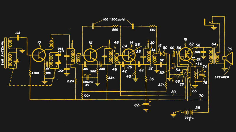
I once ran across a 6M amplifier project by a Japanese radio amateur. The passive components had illustrations I wasn’t familiar with, but because of my education/training, I had no problem reading that hams schematic. I discovered later on that, a portion of the world, doesn’t the symbols that, we in the USA use
I discovered this the other day when looking at Commodore schematics. Apparently many were drawn in Japan, where they use different symbols, in particular for polarised capacitors.
Please dont kill me… Power Point :D
Ok i got an excuse, it is the only graphic tool i can use at work. And no, it is not my job doing schematics :P
The most beautiful schematic I ever saw was made in Excel.
p̶i̶r̶a̶t̶e̶d̶ ̶c̶o̶p̶y̶ ̶o̶f̶ ̶P̶h̶o̶t̶o̶s̶h̶o̶p̶ ̶C̶S̶5̶ MS paint
I’m mostly joking, but I really just use pen and paper and then scan it in and move bits around if I need to do some major redesign of some sort. I mostly make automotive circuits so they’re simple enough to not need like… trace layout tools and shit. I know, I’m a dirty unwashed plebian. I am aware of this.
Don’t feel bad. I’ve made spreadsheets do things not normally expected.
On Reddit a few years ago, I saw a video (or DVD?) player built in Excel (using VBA and some Windows libraries) because that’s all someone had access to at work.
I use Inkscape with https://commons.wikimedia.org/wiki/File:Electrical_symbols_library.svg
I enjoy using diptace, i transitioned from national instruments ultiboard which i thought was good. When i left uni and stsrted my own business i needed free or licenced tools. So i tried kicad and disliked it, eagle at the time went cloud based so i decided to try diptrace and ended up purchasing it.
PCAD 85 for capture and schematic. It is DOS based. Everything is editable through text files.
I been using OrCad since the early 80s. Would never use anything else. Its the industry standard.
Not in our industry…
I use gEDA all the way to the fab. I don’t often publish schematics but when I do, I use the “Write image” feature to export to Encapsulated Postscript like [this](http://hobby-electrons.sourceforge.net/tutorials/gEDA/index.html#Publishing%20schematics)
Finally, gEDA pops up. Love Schematic and PCB
Kicad and Eagle… By Cadsoft not from Autodesk!
Nobody is going to say Fritzing?
Probably the most appropriately named software ever, IMO ;-)
I bit the bullet & initially muddled my way through KiCAD. Now that I have several moderately complicated & successful PCB projects behind me, I have actually become quite proficient in all phases of design & documentation using KiCAD. I agree with Joel (above) in that I make extensive use of the parts libraries available from Digi-Key. These two capabilities together make for a very powerful pair. My customers & my fellow engineers are both perfectly happy with the output (complete schematics, as well as production PCB w/ very useful & informative silkscreen).
Visio.
I’m a hardcore Linux user these days, but Visio is the one place where there is no reasonable alternative. Visio is not without its (dramatic) faults, but the inability to produce conceptual drawings that aren’t overly cluttered or adjust presentation without drawing the result into another editing tool rules out nearly everything else. Inkscape is probably the best alternative, but the lack of an interface to accommodate a parts library (even if I make the parts myself) makes it a pretty heavy handed kluge.
Have you tried LibreOffice Draw?
For schematics with simulation, I’ve used Oregano. Once I modeled a 1 megawatt VLF antenna tuner. For analog ICs, I used to use LTspice but there’s no Linux version, and of course they don’t have parts I used a lot, like, you know, high power klystrons.
For schematics and board layout, I’ve ordered many PCBs using expresspcb on Mint using wine.
I think LTspice runs ok under wine. I tried several circuit simulators under wine once and my memeory indicates that this was the one which suceeded.
Mechanical pencils, graph paper, and a straight edge. I use coins to create outlines for tubes. I would like to find an electronic drafting program that would spit out a schematic that looks like it was created in the 50s in terms of symbols and layout. Revising paper schematics as you go gets pretty tiresome. Either it involves a lot of re-drawing, or I copy it with paper blanking out the stuff I want to remove, then draw in the modifications in the empty spaces.
Draw it in LibreOffice draw, then save as a bitmap. Open in gimp, then add blurring and noise. Scan in a piece of paper with a coffee mug stain and overlay it. Rotate a few degrees then threshold to get that xeroxed 3 times look.
Well, if you really want to draw them the old fashioned way… How about the schematic at the top right of this page (http://sunrise-ev.com/controllers.htm)? Or, the animated schematic at the top left of the same page?
KiCAD because:
It’s available for all major platforms
The license is really free
Your content isn’t tied to a website that might go away (where are your Google+ photos now?)
It works pretty good
It’s reasonably easy to use (at least no harder than Eagle)
If you played with KiCAD a few years ago – and found it difficult / quirky – give it another shot. Recent releases are vastly better.
KiCAD – it’s just fine!
I am a Altium user for about 9 years.
I hated KiCad 4. I think 5.1 is big improvement. KiCad needs a better stack up manager and a way to scrape part data from Digikey, like Altium has. That’s mostly what I miss from Altium. I use KiCad for home projects now.
Who is going to be the first one to admit they use Fritzing?
I’ll cast another vote for Fritzing, I think that makes three of us.
http://fritzing.org/home/
Been using Draftsight for the last few years, but that will come to an end at Xmas.
Dassault have no free version of Draftsight 2019, and will disable the free version of 2018 on 1/1/2020.
I’m a big fan of Draftsight at home and work and I was disappointed by this news too. I do just enough 2d dwg work for it to be a pain not to have it, but by no means do I do enough to justify a standalone Autocad license. For work, my solution came by way of being purchased by a larger company which had volume Autocad licensing. But for home, I’ll be switching to librecad. If you haven’t tried it in a while, it is worth a second look. DWG support is still a little wanting but take a rainy day between now and Christmas and save all your stuff as DXF and you’ll be set.
Altium Circuitmaker…
Using Altium Designer (Protel 98 when i started) for over 20 years professionally. So the easyest and most logical way for me was to just use the free offering for home projects.
The “cloud library” is annoying the heck out of me, but i can work around the weaknesses with some tricks.
https://hackaday.com/2015/10/05/the-worst-cad-package-ever-is-still-handy/
First started with OrCAD in 2001, then switched to CADSTAR which was a big improvement at the time. When I left the company, I started to use Eagle because it was widely used in the DIY community (Arduino, etc). Tried KiCAD once, it was a horrible interface at that time, maybe I should try it again now.
Now that Eagle has been bought by 3DS, it will most certainly loose it’s free version, as Draftsight just did.
I recently tried https://easyeda.com/ which is full cloud based (software in browser). Seems nice at frist, I need to dig into it.
Eagle got bought by Autodesk, not 3DS, I’m pretty sure.
In early stages for small things I will still use pencil and paper myself. Maybe it’s a generational thing but to me until a certain level of complexity is reached hand drawing just seems so much more natural and convenient than any computer program can hope to be.
Once I reach the point of using a computer it’s KiCAD all the way. I noticed from a lot of people’s comments that they have different tools for different situations. Mostly one they like if they only want to publish a schematic vs another if they need to export a netlist and create a PCB. I can sit down and stumble my way through making a schematic in anything. But to really become good at it takes time and work. I’d rather just use one tool that does all the jobs I might need and try to become as good at that tool as I possibly can.
Ok, this isn’t a tool or method for drawing schematics but it’s kind of related and too much fun not to share.
How about a set of “stylized” schematic symbols to liven up your diagrams a bit? Ever since I first saw this I have been meaning to add these symbols into a KiCAD library. I guess nothing stops one from doing the same with Eagle, Altium or whatever if one is confused like that.
https://ludens.cl/Electron/audioamps/aaaa.html
Black gel pen, drafting templates, 5×5 ruled graph paper. Then move to over to software. They all horrible creativity crushing eye straining wrist tunnel burning horrid made in hell by Lucy himself.
Oh and Fritzing not bad.
Fritzing is not bad if you want to hook something up; get a visual wiring diagram. If you want to understand a circuit, it looks pretty useless.
Fritzing Not a Spice program anyway. Yet. I wouldnt go as far as ‘useless’. It does have another two tabs although some of its’ models dont have a completed section for the other two tabs. Incomplete visual models only(first tab).. Most incomplete are from users who really dont want or need more than visual representation. Again Yet. Some are screwed up alphas not used or tested. Like many of the programs the build of model (component) and its relevant accuracy is key to the usefulness of the program. The larger the library of accurate models the better. Making it easier to make those models would help.Fritzing is lacking. In my babbling on about this the relevant question was what programs used for drawing up schematic. Not necessarily design and simulation of circuits. A traditional iconic electronic schematic does go a long way to understanding and repairing/troubleshooting circuit.. Unfortunately some newer implementations are poor as others have noted. Labeling hell when all that is needed is a circuit line point to point. Then again some older schematics were like a childs puzzle of follow the line to the cheese amongst the other scribbles so mouse can eat. Finding the balance my need peer review.
I use this more than I care to admit: https://www.qsl.net/wd9eyb/klunky/framed.html
Wonderfully simplistic.
express pcb schematic editor is a breeze to use
I’d probably be using Electronics Workbench yet if I could find a bootleg edition that worked on Linux.
Since gEDA hasn’t been updated in 5 years, is it a) dead or b) perfect?
How does it compare to KiCAD?
KiCad is very much alive.
It is getting mayor updates, just last week it jumped from V5.0.2 to V5.1 which is another significant step in intuitive use and less weird quirks, but I have not used it yet bedause I’m waiting for it to dripple though my package manager on my linux box. Small bugs discovered in KiCad often get fixed within a few days to a week.
Some people use gEDA’s Gerbv instead of KiCad’s Gerbview beause when if KiCad should make a mistake in gerber generation, then that same mistake is likely to be made in Gerbview, but a lot less likely to be repeated in Gerbv.
So gEDA is dead?? Well, still works but no new features?
Personally, I go like this:
https://35c3.bleeptrack.de/
I have used TinyCAD ever since I moved from a company using (DOS) PCAD to one using (Win) OrCAD. I hated that so much that I searched and found (free) TinyCAD and FreePCB. There was a learning curve but after that I found making and using new symbols a breeze and that it also had the benefit that the data (for both) was held in a text-readable format ( I could process it with other programs) Since most of the time I was needing a quick turn-around for test and development the combination was ideal. I still use these programs now I’m retired. I tried KiCad and Eagle briefly but didn’t really find the need to persist.
TinyCAD is also usable for sketching but not ideal. OK if you don’t need precision.
I use Kicad and TinyCAD. If I’m doing a layout from schematic I use Kicad but if I just need a quick schematic TinyCAD is my preferred method. (I use ngspice for simulation mostly and often need a schematic to keep the netlist for simulation straight and TinyCAD is good for that also.) I find the TinyCAD symbols collection quite good and easily modifiable. Easy to pull TinyCAD schematic into documents also.
I have over the last 45 years as an electrical engineer a large toolchest of software: different tools for different purposes. If I see a nail I pull out hammer: if I see a screw I use a screwdriver.
I wish there was a port of TinyCAD to ‘nix.
M Walter
One other thing worth mentioning: If you expect to use or modify your designs years in the future, pick a CAD package with staying power. Several times, I’ve worked for companies whose CAD software was updated, and old designs suddenly became buggy or unusable.
Like word processors, CAD programs constantly “evolve”. If you pick one that is cloud-based, or requires updates or license fees, or only works on certain platforms etc. support may “go away”, making your old designs orphans that you can no longer view, much less edit. Unlike word processors, CAD programs rarely do a good job at file conversions.
Keep good paper coopies of your work. You’ll need them!
Make a copy of the binaries too when you backup your designs. Make sure the binary does not require some cloud stuff that might be gone the day you need it. No problems of course with KiCAD or other FOSS.
I make bitmap copies of schematics just in case.
As an ME, I would add that any mechanical 3D CAD parts should always get a safety copy in the form of a STEP file. This is the industry std. neutral (but dumb) file that any CAD system ‘should’ be able to open.
If you want a sketch program, use expressPCB. It’s the easiest one to learn and use.
Schematics have a purpose, they are a visual representation of a net list, they are a tool to drive a design.
I think in terms of block diagrams. They functionally describe the parts of a design. They are easier to communicate to other people, and you don’t have to be an engineer to read them. They also take very little time to draw, and define more of the “what” vs “how” for a particular feature. They help me to consider different approaches, and to assess how risky a particular design is.
If I want to draw a schematic with the intention of simulating it, LTSpice. If I want to draw a schematic with the intention to present it to others or for PCB Layout, KiCAD. If I want to draw a schematic with the intention of analyzing/designing/troubleshooting/calculating, pen and paper.