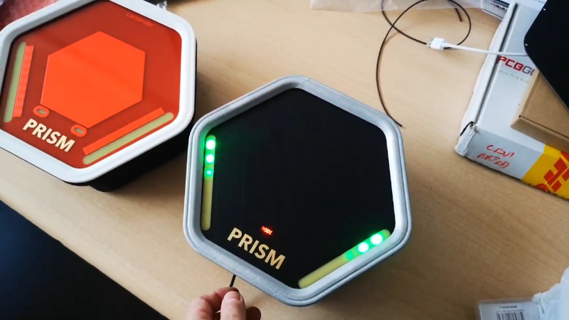
[Mastro Gippo] found himself in a pickle recently, with the development of an enclosure for the Prism electric vehicle charger. The body had been sorted out, but the front cover needed work. It had to be visually appealing, and ideally should provide the user feedback on the charging process. After some thought, [Mastro] decided to explore the possibilities of using a PCB as a part of a commerical product enclosure.
For a variety of reasons, using a specially designed PCB was an attractive solution for the team’s enclosure. Wanting something cost effective, easily customizable, and something that would help with emissions compliance, a PCB seemed like a great idea. With this in mind, [Mastro] prepared a series of prototypes. These feature see-through sections for LEDs to shine through, as well as a capacitive button and gold-plated logo. The fact that the front cover is a PCB makes the integration of the electronic components a cinch.
Before heading into full production, [Mastro] began to question why this technique isn’t used more often. Deciding to research further, [Bunnie Huang] was tapped to provide some advice on the concept. Noting that there can be issues with lead content, as well as the fact that PCBs aren’t often produced with proper regard to aesthetics, there were some pitfalls to the idea. Additionally, ESD testing can be difficult, while the in-built capacitive button would face issues in wet conditions.
None of these are showstoppers however, and [Mastro] has persevered, combining the front cover PCB with an adhesive plastic sheet for added protection. We fully expect that if more manufacturers explore this route, it may be a more viable technique in future. It’s also a great example of knowing when to ask others for help – it’s not the first time we’ve learned from [Bunnie’s] broad experience!


I give credit for my discovery of this concept to Dave Jones. I’ve been using PCBs as the front and back panels for extruded aluminum enclosures for my GPS Disciplined Oscillator (available on Tindie!) for a while now. They’re easy to design (given that you’re already good at PCB design), they can look great (depending on what you ask your fab for), and you can float a plane on them to serve as extra shielding.
nsayer: I looked @ a few of your photos to see your example. It looks like you are using “standard thickness 1.5mm” PCBs. I am just wondering how many have cracked due to mechanical / physical stress on the connectors? Especially BNC type connectors that stick out quite a ways from the surface (big torque radius) and lots of physical manhandling. As a PCB designer, I am intrigued to use them for more things where they make sense. thx! -VoltVisionFrenchy (aka Steve French).
lol what’s an IP rating? these clowns again…
If there are components soldered to the (underside of the) PCB, and the PCB is subjected to any kind of stress (e.g. buttons that can be pressed, or something could be stacked on it), then there’s a chance of bad/broken contacts to the components or traces after a while. Seems to me to be a showstopper as well, for commercially produced devices.
It’s wall mounted, so you won’t be stacking anything on it. The UI uses capacitive touch sensors and so i guess you might break some traces if you have an over zealous user, but i would imagine it would be unlikely if the board was properly supported from behind and was made of the proper thickness…
I know a guy who used to break everything he owned by pushing too hard on the buttons. One day he stuck his finger right through the screen of his TV when he missed the power button.
There are all kinds of people out there. You have to plan for the roughest ones if you want your product to last.
You can easily design ribs, perpendicular to the main pcb, to be soldered in for additional mechanical rigidity.
Be worthy of a study to find out how ‘vast’ the unsupported area can be before the repeated flexing will break solder joints or start de-laminating the board. Also if the layout on the board matter much. The idea is certainly sound but if it needs support every cm its never going to be practical with normal PCB substrates. My initial guess would be something like a mesh of supports around 5cm from each other would be sufficent.. But that really is a wild guess based on little more than a few bare boards I’ve had mounted in projects of very low rigidity.
If you are really getting clever the ribs could be a great way to make a cheaper number of layers in the board work well too.
In the case above I think a simple support around the button on the PCB so the load is pushed to the wall/case sides directly is probably all that would be needed for reasonable durability. Properly sized It would prevent even heavy handy operators from flexing the PCB where they are supposed to be interacting with it.
There are several solutions to this. Use thicker PCB material, add supports under the panel, design pcb material supports that solder on or fit in notches, add a piece of aluminum angle to the back as a brace, or hotglue some brace. Thicker material may be the easiest. Even .093 is a lot more rigid than .062
PCB’s for front panel control mounting do not hold up to the stresses from human fingers or vibration. They are highly tempting to try, but probability of failure is high, and becomes much higher if you intend others to operate it. Folks still have the attitude that if it’s not working the solution is to “Spit in the back and whomp it one!”, plus folk’s natural reaction to a device failing is to “rattle it some” to see if that’ll make it work, with tons of movies, videos, and memories of your own reactions to back that up. The military embeds circuits in potting material for just these reasons, but then repair is by dustbin and build a new one.
The problem remains outstanding enough that I’ll review every idea to solve the problem. An automatic rejection is always received for those thinking “The bigger the blob the better the job”. Lookup NASA soldering coursework for that case.
And when someone trips over the cord or a joint in the slab?
Throws out a hand and it lands on the object that they already had a mental flight plan for.
Broom handle, shovel handle, etc.
Many people tend to put lawn and garden tools in garages and lean them against -any- surface or object with no forethought of the consequences of it.
Cleaning day can be bad, as it means anything gets leaned anywhere, even if only intended to be few minutes.
one more quick scenario:
Are you carrying a small child on your hip or however? Hmm, face of charger looks remarkably like a childs toy.
Kid will probably bash it.
For bonus points they might even use that smartphone you handed them as a pacifier.
Didn’t mean to make it sound like I’ll critique ideas that are posted here. Engineers have had years and years on this problem but little improvement these last 40 yrs. Someplace out-of-the-corporate-box like HAD is just where a break-thru idea may come. We do certainly need it.
Hack on!
Thank you for your positive comment! :) We tested the design a lot and the results are encouraging, mostly due to the fact that the cover is solidly coupled to the back frame and everything is tightly screwed into a wall. We’re not using BGAs or QFNs on the cover, IC legs help to reduce stress a lot. I’m mostly worried for the ATmega crystal stability, but I can always remotely reflash their firmware to use the internal oscillator if this becomes an issue.
I can’t remember where, but I’ve seen folks using a solid piece of copper/etc.–the size of the PCB–that was routed just deeply enough to avoid traces/component/etc., then solder was used to ‘glue’ the copper to the PCB in a reflow oven. The secret was that the solder used as a glue melted at a much lower temperature that that used for the components, so they wouldn’t be disturbed. As there would be no danger of melting the component solder, you could leave the whole thing in the oven for as long as you want to make sure that everything reached the right temperature, so you could use a 10mm(!) thick plate if you wanted to. If you needed to get at the PCB to repair it/etc., you just need to remelt the glue solder and remove the plate. Even better, this would completely waterproof the entire back of the PCB. Does that make sense?
For some things I can see it being perfectly fine to have a PCB used in this way and could see some cool projects with it.
But wouldn’t see it as ideal for an EVSE for the IP ratings and not as much insulation I’d prefer a full plastic case with isolated buttons. 230V at 32A with this could end up in shocking results.
There will be plastic sheet over the PCB. The PCB itself is also all earthed ground plane, so as soon as some high voltage touches it, it will trip the mains GFCI.
Am I understanding correctly? This is a vehicle charger? Like something you are going to charge a battery up with enough energy to drive yourself to work and back?
How much power are we talking here?
And the only thing between the user and the guts is the back end of a PCB?
I’ve seen a lot of low power hobbyist projects, mostly qrp ham radios that use PCBs for their cases. That was clever the first time and not necessarily a bad choice ever since. But for projects that will be used by people other than their builders whom know what is inside and what kind of durability to expect from the case.. and it contains heart stopping levels of angry pixies?
Absolutely no way!
Eurorack community uses this idea a lot
came here to reply this =) happy patching!
Mike’s Electric stuff has also done a few video’s about PCB’s for mechanical or aestetic functions.
Some are front and back panels for extruded aluminimum enclosures.
Others are only mechanical and are used for industrial cabinets.
These usually have a steel back plate for mounting all the relay’s cable conduits and connectors (DIN-Rails).
If you have the CAD files of the Relays, etc, then ordering thick (upto 3.5 mm, maybe even more) PCB’s for use in these cabinets saves a lot of handwork with measuring the location of the holes, drilling, deburring and cleaning.