Getting your own PCBs made is a rite of passage for the hardware hacker. Oftentimes, it’s a proud moment, and many of us choose to immortalise the achievement with a self-aggrandizing credit on the silk screen, or perhaps a joke or personal logo. However, as far as artistically customized PCBs go, the sky really is the limit, and this is the specialty of [TwinkleTwinkie], whose Supercon talk covers some of the pitfalls you can run into when working at the edges of conventional PCB processes.
[TwinkleTwinkie]’s creations are usually badges of one type or other — they’re meant to be worn on a lanyard around your neck, as a pin, or as a decoration added to another badge. The whole point is the aesthetic, and style is just as important as functionality. With diverse inspirations like Futurama, Alice in Wonderland and the shenanigans of the GIF community, his badges blend brightly colored boards with a big helping of LEDs and artistic silkscreening to create electronic works of art.
Keeping PCB Fab Houses from Upsetting the Artwork
These days, PCB fab houses offer more choice than ever, in terms of silkscreens, soldermask colors, and other options. However, fundamentally, their primary concern is to produce reliable, accurate, electronically functional boards — and it’s something that can cause problems for #badgelife hackers designing for more aesthetic reasons.
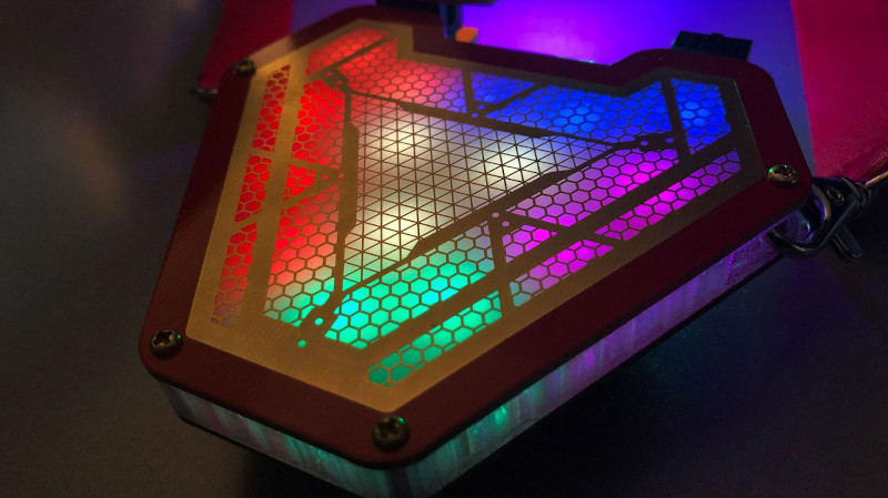
[TwinkleTwinkie] ran into this very problem during the development of the Arc Badge, a piece designed to replicate the famous arc reactor from the Iron Man and Avengers films. The basic idea of the badge was to have a base PCB which carries all the hardware, along with a spacer, and then a third top layer consisting of a PCB which the LEDs were intended to shine through. The prototype board worked well, with the fab house producing it on 1.6mm thick FR4 with white silkscreen and red soldermask. For the final product, wanting something a little fancier, black silkscreen was chosen instead. Ordered through PCBWay, this necessitated using their “Advanced Production Fab”, and a longer lead time, but after a few weeks the boards were ready.
Unfortunately, despite looking great with the black silkscreen contrasting with the rich red soldermask, there was a problem. When [TwinkleTwinkie] asked for black soldermask, this also led to a change in FR4 material, to a different grade which was more opaque than the prototype board. This led to the LEDs showing up very dim, and spoiled the visual effect that was desired for the ArcBadge. The dimming was so significant that users would no longer get the glow-through effect when wearing the badge under a T-shirt, a la Tony Stark. It took comparison with the prototype to figure out what had happened. PCBWay had simply used a higher-grade material when switching to the black silkscreen. Given that PCBs are sold as electronic products, and not for their optical qualities, they hadn’t done anything wrong, per se – but regardless, the new boards weren’t fit for purpose.
Order, and Order, and Order Again
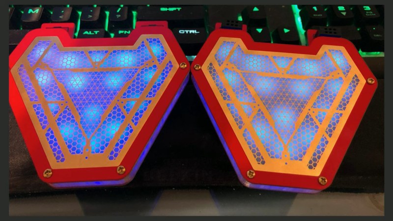
The solution was simple – the boards would need to be reordered. In order to guarantee the LEDs would shine through and be truly resplendent, precautions were taken. The final board switched back to white silkscreen. As an additional precaution, in case PCBWay kept using the new material, the new part was instead 0.8mm thick, allowing it to block less light.
The redesign left [TwinkleTwinkie] with 250 coasters to give out, but his commitment to giving his customers a quality product is commendable. Despite nobody outright making a mistake, the final product would have been a little disappointing had the redesign not taken place. The Arc Badge, as delivered, glows with the best of them, and we’re sure everyone involved is wiser for the experience!


On one hand I’ve very much into this and do it myself on the other hand its a complex skill that no employer values
Okaaayyy… I get that the idea is to create artistic PCBs, but since the top plate of the Arc Badge doesn’t actually contain any circuits, wouldn’t it be a heck of a lot saner & more reliable to, say, UV print the image on a piece of laser-cut frosted acrylic?
Artistic PCBs are glorious and all that, but perhaps they would best be used for, well, PCBs,
In practice PCBs are so much cheaper than any other form of digital manufacturing (maybe barring home 3d printing) that you kind of need to consider them as an option regardless of how suitable they are.
Printing and cutting acrylic sheet would likely cost 10-100x more than the PCBs.
pcbs are cheaper than anything you are thinking of by an extreme margin
Another potential problem with transparent PCB’s is that some manufacturers put their brand name or other marks into the FR4 (Under the copper).
I think this was mentioned in another Hackaday article of Arty PCB’s a few years ago.
I know that most people wouldn’t anticipate such a small change (silkscreen color) would change other aspects of the board, but there’s always a risk when making any change with your first production order. A cautionary tale worth sharing, and kudos on him for not just going with it.
Pretty sure you could talk with PCBWay or any other mnufacturer if you want a specific layer stackup with core and prepreg material (weave, glass content, epoxy resin, …). It might probably cost you a few bucks more to have a fully specified stack produced, but still sounds better than having 250 trash coasters produced just because you decide to do an unspecified production run in the hopes the manufacturer will magically dream up what ever your design intent was and not change anything along the way.
The hard part is definately to find out the optical properties of the different cores and prepregs out there, maybe asking some of the laminate manufacturers would be a nice idea to start, they definatey have some samples laying around and mybe even have a few hints to point you to the optically clear materials.
As an electrical engineer, what this story tells me is that people need to be more meticulous in creating their fab drawings. If you just send a board house the gerbers, you’ll get whatever material they have on hand, but if you create a proper fab drawing you can specify your exact stackup, layer thickness and whatever material you want used including whatever properties you want whether they are electrical, optical, mechanical, or anything else. You might pay a bit more if you overspecify but you’ll get what you want.