Here at Hackaday we love projects that are so well-documented that you can spend days reading up on what the designer has achieved. [John Lonergan] didn’t disappoint when he designed the SPAM-1, an 8-bit CPU built from discrete logic gates. His detailed log contains a wealth of information on such things as designing opcodes, optimizing program counter logic, running a digital simulation, as well as his thoughts on microcode design. The sheer volume of it may be a bit off-putting to beginners, so it might be best to start with the video series that describes the architecture and goes into detail on several sub-blocks.
The design has changed a bit since [John] first started on the project, as he decided to add more and more features, but the final result is a well-thought out architecture that keeps the simplicity needed for discrete hardware but still has enough features to keep it interesting for seasoned CPU aficionados. The instruction size is rather large (48 bits) to simplify the instruction decoding at the expense of larger code size. Conditional jump instructions are not present; instead, all instructions have an optional control flag to make them conditional, a feature inspired by the ARM instruction set.
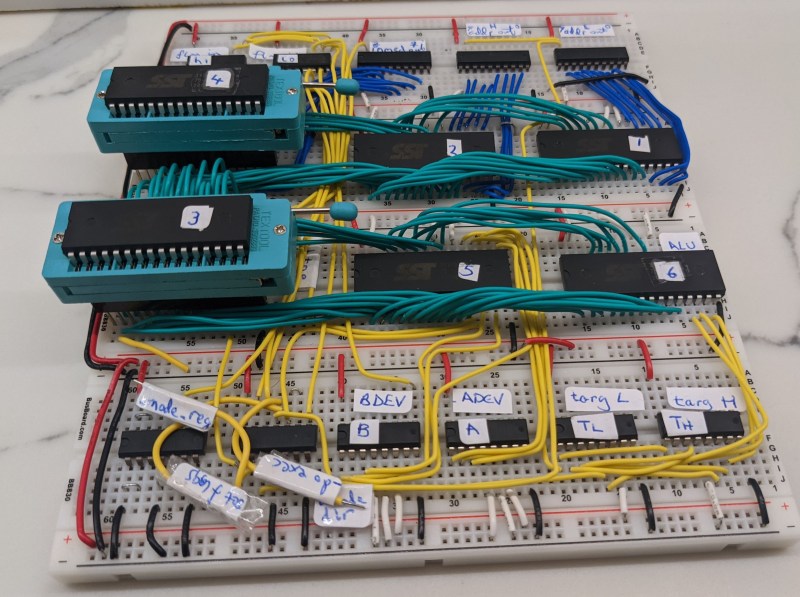
Once the design was mature enough, [John] modelled the entire thing in Verilog and simulated his design to verify correct operation and to check the timings, estimating it to be workable up to 5 MHz or so. A large stack of breadboards and DIP chips from the 74xx series then brought the design to life.
Not content with simply designing, simulating and implementing a custom CPU in hardware, [John] also spent significant effort on the software side of things, writing an assembler and even a C-like compiler for the SPAM-1 platform. And if that wasn’t enough, he also added an emulator for the classic CHIP-8 language, which allows it to run existing programs like Pong and Tetris. Input and output for all this software is mostly through a UART connection to a PC. A VGA interface is still on [John]’s to-do list, but he did build an adapter to connect a classic NES controller to the system.
The SPAM-1 is a worthy addition to the long list of discrete-logic CPUs we’ve seen here, such as this breadboard computer running a UNIX-like OS or this minimalistic one. If you’d like to see one that implements an existing instruction set, try this homebrew RISC-V computer.


Whew! Just in time to save humanity from the forever chip shortage.
Wow! Thats a lot of (SST) 128K flash ROMS for an 8bit CPU!
Yeah, It’s like a “poor mans FPGA” here. Lots of large look up tables at the expense of speed (Logic propagation delay (x ns) vs FLASH access time (xx ns).
It kind of takes away the “logic” understanding of instruction decode and implementation. But it vastly reduces chip count and the complexity is now in the FLASH instead of wires and gates.
I’m tempted to do something with a couple of 74181’s or a custom gate CPU (too many chips and breadboards lol).
The big advantage of FLASH driven microcode is that you can hardware emulate another existing CPU and then you have an instant codebase.
Yes, Flash and eepROMs (typically faster access times compared to Flash) are indeed the poor man’s FPGA.
Or for those who don’t want to deal with all the paperwork surrounding getting the software tools for programming an FPGA or CPLD.
>paperwork surrounding getting the software
https://symbiflow.github.io/
Symbiflow has its pros and cons.
It is a bit of a hassle to get it up and running. Since it requires some software knowhow, especially when it comes to Linux knowledge.
Its device support is getting better with time thankfully enough. But it has a bit of a sharp focus on higher end devices and lackluster support for the lower end of the market.
But yes, Symbiflow is a lot less paperwork than an IDE from an actual device maker at current. But it still has a long way to go before it is a decent tool.
I just had a look around at what I can get in my country in DIP.
Seems FLASH is the better option at about 40ns.
Looks like the fastest way is to start with FLASH and then shadow it onto SRAM which gets down to lower access times in DIP.
It’s a big regret for me that I waited so long to get over that barrier.
I started with a CPLD development kit by Vantis that had several MACH2 CPLDs.
Early days then the devices had only 32 or 64 macro cells so they were like the next step after the common 22V10’s.
Anyway, I never succeeded in getting a license key for a paid educational development kit so I gave up completely.
The next attempt was decades later. I bought a Papilio FPGA educational platform.
I think it had it’s own IDE but I used the Xilinx platform instead.
The Xilinx platform (ISE) was a pain in the ass to get a key for and then it didn’t work without some tweaking of some text files to adjust file location pointers.
Altera was much easier, still hard to get the license key but the software worked out of the box.
Now days the are freeware open source alternatives. So there are no excuses.
I see one linked to above. I havn’t used it but my comment would be that is “seems” to lack support for simpler, cheaper and importantly less expensive devices and only supports more recent devices.
You can still pick up more hacker freindly CPLDs for learning with on eBay (some no longer in production) like Xilinx XC9536XL / XC9572XL / XC95144XL CPLDs which are 36/72/144 macros, 5V tolerant 3.3V chips or Altera EPM240 / EPM570 which are 240 / 570 LEs or about 190 / 220 macros approx and are 5V tolerant with series resistors. Both of these series have package outlnes available that aren’t to hard to solder like 0.5mm QFP. There are some modules available per-assembled on eBay.
Not so sure about the poor man part as CPLD/FPGA are more cost effective for their gates. You can buys a FPGA board with enough gates for $20 these days if you look around.
Question is can you then actually do something with them – FPGA tools can be rather expensive, not all of them are supported by the open tool chains etc… Also have to learn HDL to actually make them do something, which isn’t too bad in many ways, but is another step on just understanding how it works.
Not that I disagree, FPGA do seem like the obvious choice for most of these projects in a boring and practical sense… And at some point I’ll really finish learning and do some things with FPGA, when I can actually afford the FGPA of the scale needed for the projects I have in mind…
Both Xilinx and Altera have free IDE’s. These free IDE’s wont do all devices but they do do anything a hobbyist or hacker is likely to use. There are also open source alternatives.
Modern FPGAs have absolutely huge gate counts. Most tasks will fit into smaller and cheaper FPGAs. Many tasks will even fit into smaller and cheaper CPLD which also have higher gate counts now.
If you want to learn to use a FPGA/CPLD IDE and to learn a HDL, I recommend starting with a cheaper CPLD. The process is the same and line between CPLDs and FPGAs has blurred so much that you can just think of FPGAs as larger CPLDs.
Hi the ROMs are not microcode as such; it’s pretty much a horizontal encoded CPU so the ROMs are simply the program memory of this Harvard CPU. The decode logic is just a few 74138 decoders hanging off the ROMs to decode which devices are selected for read and write.
At a stretch any horizontal encoded CPU can be considered as having every instruction as a microcode op, but I thinks that’s a stretch here.
It’s the program memory that’s all.
In a similar vein is Magic-1 by Bill Buzbee: https://www.youtube.com/watch?v=qOcSnaK0yBw
Question:
Where to buy fast SRAM / PROM (FLASH ; NVSRAM etc) in DIP?
I am in Australia and the best place seems to be element 14 : FLASH 40ns , SRAM 12ns
I have a pile of old 74xx chips. Would anybody need them?