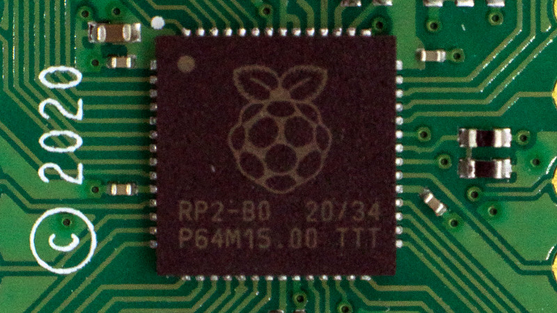
[Dmitry Grinberg] is an adept tinkerer who wanted a much larger RAM space on his Raspberry Pi 2040 (RP2040) than the measly 264kb on-board SRAM. The chip does support 16MB of off-flash memory via a QSPI bus, but this must be accessed explicitly rather than being memory mapped. With clever trickery involving XIP (Execute in Place), Dmitry mapped 8MB of external QSPI RAM into the address space.
XIP mode allows the chip to fetch data on-demand from an external chip and place it into RP2040 caches mapped at 0x10xxxxxx. The RP2040, although incredibly versatile, has a limitation – it can only perform read and execute operations in its XIP mode. The first step to solving this was to get data from persistent storage to RAM on boot. Armed with a dual-OR gate IC, an inverter, and two resistors, [Dmitry] can toggle the nCS pin that selects between flash and RAM. A first-stage bootloader copies the program from flash to RAM, then sets up XIP mode and launches into a second-stage loader.
Of course, glitches couldn’t resist making an appearance. The RP2040’s GPIO IP block doesn’t reset properly, so the nCS pin doesn’t go back to selecting flash after reset. For [Dmitry], it wasn’t a problem as he used an I2C IO expander and made the troublesome pin dance to his tune.
The next step was to write changes back to RAM when the cache was flushed. This is where the MPU (Memory Protection Unit) gets abused. Usually, a write to 0x10xxxxxx will flush the cache line. When a write happens, the MPU can trigger a hard fault by marking that region as read-only. The handler emulates the write instruction and flushes the cache line. From a high level, it seems pretty straightforward, but there are 127 different types of write instructions for ARMv6M. While most code is read-heavy rather than write-heavy, performance is still a concern. Luckily for him, memcpy clocked in at 36 Mbit/s at stock clock rates, a commendable achievement given the inherent challenges.
[Dmitry’s] groundbreaking code is accessible for download on his website under a BSD-2 license, allowing others to explore the potential of vast amounts of RAM on the RP2040 microcontroller. This innovative approach opens doors to all sorts of creative possibilities. Despite being a partial ARMv6 emulator, this isn’t the first emulator we’ve seen on RP2040, as this RISC-V emulator attests.


nice
So basically the XIP can run code either in sram or external dram but not both? At 363 clock cycles per write it’s a big compromise vs writing to sram (couldn’t find how many clock cycles, but writing to cache takes 1 cycle, I’d imagine writing to sram takes less than 10 cycles?). At over 30x slower, if the application doesn’t need fast writes then it’s fine.
You’ll also loose using dma being able to write to sram through 4 channels from various peripherals with the dma bus capacity of up to 2Gbps.
But it’s an impressive hack none the less!
I want to make clear what XIP (eXecute In Place) means in RPi Pico world: fetching the code from the flash memory, copying the instructions directly into the cache. the non XIP/the normal way is on boot copying the code from flash to the internal sram and then fetching the code from sram into the cache for execution.
In other words, you are not supposed to be able to write to the XIP memory, just read from it, unless you start in flashing/boot button mode.
I am guessing that this hack has something to do with his previous hackaday appearance: https://hackaday.com/2022/07/14/a-linux-business-card-you-can-build/ But it is just my guess.
Reading or writing to SRAM on the RP2040 only takes one cycle – the cache that he’s talking about in this article is in the RP2040’s SRAM.
just page, bro. EMS forever :)
Doom on a pico?
Graham Sanderson implemented a completely uncompromised version of Doom on a Pico without needing external memory: https://kilograham.github.io/rp2040-doom/
Wow thanks
Hm..okay, this is probably a nice exercise for a student, but why?
The biggest problem of our time is not that 264kb of Ram is not enought,
it is the high amount of bloatware from people that believe that they realy
need more and never learn that they can solve there problems with 1/10 of the
resource they using now.
Thinking about a bigger computer for the next year? :-)
Dmitry is using this to run Palm OS on the RP2040, check out his rePalm project!
https://dmitry.gr/?r=05.Projects&proj=27.%20rePalm#_TOC_0734fd58b98b17e23027547eec1258f5
is a direct link. And the need to support self-modifying code in various guises likely drives some of this.
I’m not sure I completely understand the problem he is solving. Is the RP2040 not capable of interfacing to external RAM on the QSPI pins, or is it just that he wants to be able to do XIP on the external RAM? I ask because I’m thinking about implementing a really cheap display controller using an RP2040, but 264kB isn’t enough for even an 800×480 framebuffer, which is 1.15MB for 24-bit color or 768kB for 16-bit color. I don’t mind if I have to first copy the firmware to internal RAM, then switch the QSPI CS to the external RAM device, but the RP2040 memory manager is a bit mysterious to me. I’m not quite as smart now as I was back when I knew everything.
Yes, you can interface with external RAM but you’re just talking SPI to it. It’s not memory mapped. That is the problem he is solving.
I have a Pico-based project (Gravis Ultrasound emulator) that needs 1MB of sample memory and the problem is constrained enough that a simple interface that can peek/poke bytes into SPI RAM is enough for me, but this is a really interesting hack that opens up a lot more possibilities.
That’s not fully correct (HaD post is a little unclear too): the external PSRAM is memory mapped, but only for read (and thus execute) accesses. Of course that makes the “write” part of RAM somewhat unusable. Dmitry uses MPU to trigger “manual” write using exception for address-mapped write access to this region.
I’ve considered doing a virtual machine that abstracts gpio as memory mapped ram but that would be slow as hell
It may be worth considering an ESP32 with PSRAM. It’s easy to use and works with lvgl.
Pimoroni have recently released a graphics co-pro type system with a Pico-W onboard that uses a second RP2040 with 8MB of PSRAM for double-buffered frame updates. As yet they haven’t released the schematics but there’s plenty of info on their site about the implementation.
well done!
It’s worth pointing out previous work in this vein, [AsuMagic]’s SPI PSRAM access for the yocto-8 project, back in 2021:
https://forums.raspberrypi.com/viewtopic.php?t=316012
Instead of using the MPU, that solution uses unmapped adress space and traps both reads *and* writes through the HardFault handler. No provision for execute, though. Accesses are backed by the usual SPI peripheral and a software-based cache.
Prof. Salamander’s assignment: Use binary rewriting (or even play around with the compiler) to have the program call your external RAM handler directly instead of trapping and emulating accesses at runtime.