The synthesis of single-atom layer versions of a range of atoms is currently all the hype, with graphene probably the most well-known example of this. These monolayers are found to have a range of mechanical (e.g. hardness), electrical (conduction) and thermal properties that are very different from the other forms of these materials. The major difficulty in creating monolayers is finding a way that works reliably and which can scale. Now researchers have found a way to make monolayers of gold – called goldene – which allows for the synthesis of relatively large sheets of this two-dimensional structure.
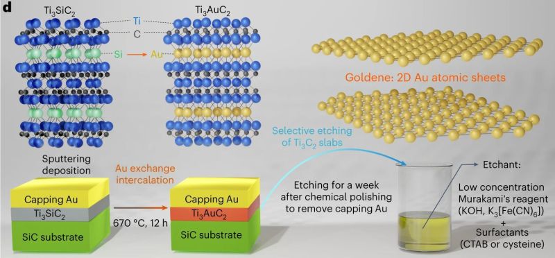
In the research paper by [Shun Kashiwaya] and colleagues (with accompanying press release) as published in Nature Synthesis, the synthesis method is described. Unlike graphene synthesis, this does not involve Scotch tape and a stack of graphite, but rather the wet-etching of Ti3Cu2 away from Ti3AuC2, after initially substituting the Si in Ti3SiC2 with Au. At the end of this exfoliation procedure the monolayer Au is left, which electron microscope studies showed to be stable and intact. With goldene now relatively easy to produce in any well-equipped laboratory, its uses can be explored. As a rare metal monolayer, the same wet exfoliation method used for goldene synthesis might work for other metals as well.


Isn’t this done all the time? I think it is called Chemical Vapor Deposition (CVD).[1] Getting atom-scale deposition thickness is common.
1. Chemical Vapor Deposition (CVD)
https://en.wikipedia.org/wiki/Chemical_vapor_deposition
I don’t think this is done with Gold through… at least nothing describes this for gold in this article…
There’s definitely other types of gold deposition but I don’t think they can do 2d sheets of it. hopefully someone knowledgeable can bring a response there
Yup you may be right. Maybe what I’m thinking about is Physical Vapor Deposition (PVD). I seem to remember reading about (PVD) gold plating plastic parts at or near atomic scale thickness so the cost per part is very small yet the plating is robust enough to last. In PVD I seem to remember gold (or some other material) was “sputtered” as a plasma in a partial vacuum chamber. Maybe someone with real PVD/CVD plating experience can fill in the gaps.
The first step in the graphic is labeled “sputtering deposition” so you’re right about that, but the innovation here is the method of separating it from the surface it’s deposited on while maintaining the integrity of the sheet. I’m not sure what the benefit of that is, but that’s what they’ve accomplished.
I believe the problem was that gold atoms tend to clump together (presumably in multiple layers) before a single layer can form when any “normal” deposition is done. This method doesn’t use the “capping gold” directly but allows the gold to replace silicon in the TiSiC layer, creating a single layer of gold between the TiC layers, then etches away the TiC layers leaving the single layer gold intact. FWIW
They missed an opportunity there. Surely “Aurene” would have been a better name?
Time to stop doing wedding rings from gold.
Why?
What are the “interesting properties”?
A more efficient antenna? How much area can I cover with how much gold?
Nice! Just gotta train it a bit and evolve it into Seaking!
https://pokemondb.net/pokedex/goldeen
“Goldene”? Gah.
I could live with “aurene”. Ugly, but at least it’s not “goldene”. Ugh.
“Goldene” is a terrible term. Graphene refers to graphite and double-bonds (ene).
Goldene was “Jolene’s” sister.
You see that kind of thing too often.
Like how they named the LASER version of the ‘iron dome’ defense system ‘iron beam’… I mean iron? Really?
Isn’t goldene a pokemon?