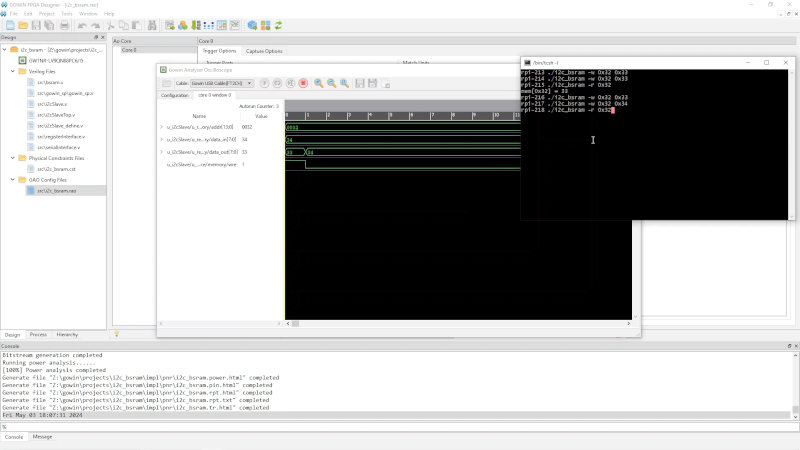
[Grug] has been working with the Tang Nano 9K FPGA board. He wanted to use the Gowin Analysis Oscilloscope (GAO) to build an internal monitor into the device for probing internal points. The problem is that the documentation is a bit lacking, so he made a video showing how to make it work to help us all out.
The idea for this isn’t unique, although for some vendors, getting this capability requires you to buy a license or the free versions are limited. We were disappointed, as was [Greg], that he had to run Windows to get the software to work.
The software seems capable, although we were interested in how much of the chip’s resources the integrated logic analyzer uses. We know from experience that being able to have a bird’s eye view of the signals inside the FPGA greatly simplifies debugging.
The Tang boards contain GWIN-1 FPGAs with different gate counts. We assume this software will work with any of the devices, regardless of the size. We’d love to know how to make this work on Linux, even if it takes a VM or WINE. In addition, the program has a number of options and features that either don’t work or aren’t clear what they are supposed to do. If you have any insight on any of this, be sure to share it with [Greg] and the rest of us.
We’ve rolled our own version of this that is portable. We’ve looked at this FPGA before and it is dirt cheap.


I’d also like to mention Project Apicula 🐝: bitstream documentation for Gowin FPGAs
https://github.com/YosysHQ/apicula
Just bought one of these, waiting for it to arrive. Plan to play and learn FPGA along the way.
Be nice if AMD built a FPGA chiplet into their CPUs.
Not really: FPGAs themselves are pretty poor usages of silicon space, which is why an absolute top-end process FPGA still is dramatically limited speed-wise comparatively. Hence the reason why the reverse (FPGAs with hard CPUs inside) are still so limited speed-wise. I’m not saying it wouldn’t be *useful*, just a big cost increase for anything capable.
Part of the reason why AMD and Intel bought Xilinx/Altera was because the design teams were some of the fewest in the world working on absolute top-end processes, so the actual devices were less interesting than the talent.
Yes, the flexibility of FPGA logic comes at a cost, but no FPGAs are not “pretty poor usages of silicon space”. You don’t understand the trade-offs. FPGAs allow something much closer to a custom hardware solution for customers who cannot afford a full custom ASIC. The faster clock speeds of CPUs and GPUs are often no match to this. FPGAs offer far greater parallelism. FPGA solutions often beat the next best programmable thing by a couple of orders of magnitude especially in performance per Watt.
The idea that Intel would pay $17 billion for Altera or AMD would pay $49 billions for Xilinx just for the talent is laughable.
“You don’t understand the trade-offs. FPGAs allow something much closer to a custom hardware solution for customers who cannot afford a full custom ASIC.”
I mean, given that I literally have been involved in whether or not to create a custom ASIC vs use an FPGA design when we had both designed, I’m pretty sure I *absolutely do* understand the tradeoffs. (We went with the FPGA for the digital portion and had the ASIC be mostly analog, incidentally).
The reason why an FPGA design can actually end up more power-efficient is because FPGAs are built on the absolute most modern processes, and you don’t have access to the top-end processes with custom ASICs. So you win out because even though you’re effectively wasting a *ton* of silicon (and power!) on the interconnect and routing, it doesn’t matter because the process shrink wins it back in spades: you’re not comparing “16 nm FPGA vs 16 nm ASIC” you’re comparing 16 nm FPGA vs 130 nm ASIC.
But when you’re talking about CPUs, you’re not talking about old processes anymore, and it’s apples-to-apples. The die space *on the CPU* is more valuable *for the CPU* at that point, because you need to dedicate a *lot* of die space for the programmable interconnect.
This isn’t rocket science: any given net in an FPGA routes through dozens if not *hundreds* of interconnects, all of which have transistors that you’re driving: on an ASIC that’s just a metal wire. You can flat-out see it in the FPGA itself! The DSPs and block RAM in pretty much any given FPGA have *dramatically* higher power and space efficiency than the interconnect fabric.
Again, please note what I’m saying – I’m *not saying* that an FPGA-style interconnect couldn’t be *useful* in a CPU. I’m saying that the die space you’d need to dedicate to one to have one be useful is too large and would push it cost-wise out of market.
Actually, let me TL;DR that:
If you’re comparing performance/Watt for FPGA/CPU/GPU/ASIC all on same process nodes, the ASIC’s always going to win. The FPGA will do pretty well, but *only because you’re using the internal hard blocks* – if you tried to do it in interconnect only, it’d be god-awful! Which means the advantage you’re getting is just due to the fact that the parallelization available in CPUs/GPUs doesn’t match your workload yet.
The issue is that in order to make the FPGA portion big enough to be useful to be on-die for a CPU, it’d be too big. For any fixed application you’re far better off in straight silicon, and to gain the programmable advantage you need much more than a “chiplet.”
“lattice fpga fig forth”
https://www.google.com/search?q=lattice+fpga+fig++forth&sca_esv=7fd248ba2150affe&sca_upv=1&sxsrf=ADLYWIKyHJLZYNM8G9LDwCPiD4efxA0iXA%3A1715085896001&ei=RyI6ZuPgPNu10PEPqeiDkAc&ved=0ahUKEwijoNzsyPuFAxXbGjQIHSn0AHIQ4dUDCBA&oq=lattice+fpga+fig++forth&gs_lp=Egxnd3Mtd2l6LXNlcnAiF2xhdHRpY2UgZnBnYSBmaWcgIGZvcnRoMggQABiiBBiJBTIIEAAYgAQYogQyCBAAGIAEGKIEMggQABiABBiiBDIIEAAYgAQYogRIw3JQtRdYlFpwAXgBkAEAmAF8oAGBBaoBAzIuNLgBDMgBAPgBAZgCB6ACkgXCAgoQABiwAxjWBBhHwgIHECMYsAIYJ5gDAIgGAZAGCJIHAzMuNKAHwBg&sclient=gws-wiz-serp
fig Forth has
1 ENCLOSE
2 BUILDS>
3 State-smart words
Changes made to fig Forth in attempt to damage it?
” Lattice fig Forth”
fig Forth has
1 ENCLOSE
2 BUILDS>
3 State-smart words.
The 20K is interesting, there’s development work going on for a MISTeR like platform, but lso singular projects especially C64 & Atari ST are going now. It’s got an SD card slot built it, and working being done on making the on-board BL616 work in USB-OTG mode, whilst still allowing for USB-JTAG reflashing of FPGA, although you can get cheap USB-OTG working with an inexpensive Sipeed M0S, which is basically just a seperate BL616, and there is verilog code to link it into the FPGA.
20 quid or so to emulate most 8bit cores isn’t bad at all :-)
Careful with the Tang FPGAs… there’s some evidence to suggest that if they get pushed too hard, they just sort of… don’t work properly.
See https://github.com/juj/gowin_flipflop_drainer
Buried deep in the reddit threads there seems to be evidence that the issue is related to the particular 1.0V regulator used on the boards, along with its capacitors. So , its not a fundamental issue internal to the FPGA itself, but something that is affected by and can potentially be mitigated by better on-board core power regulation.
The Github repo tries to claim that this is “disproven,” but you usually can’t fix simultaneous switching noise by just changing the values of capacitors, because the inductance stays the same since the packages are the same. It’s a board design issue, you just need lower inductance.
That being said, the fact that it’s speed related (and the scope traces) actually tends to point to a timing failure closure, which wouldn’t surprise me at all. The “but it meets timing according to the tools!” comment is fairly hilarious – you think the software is perfect but the hardware is bad?
Hell, it’s not easy to ensure that the *major* vendor tools work properly when it comes to timing!
The “there’s crosstalk between the onboard flops” is far, far easier to test than this oddball test – just instantiate a bunch of LFSRs offset in the start point (so all the flops are toggling differently), delay the outputs of each to line up, and check to see if the outputs are all identical. Given the simplicity of LFSRs you can basically fill almost the entire chip. Even if a test like that fails, though, it’d probably point more to a supply issue – it’s entirely possible the *chip itself* doesn’t have enough power/ground pins or they’re not distributed well (this was a common problem on early FPGAs).
Not sure what was that “wish we could do it on Linux” about. Gowin ships native Linux version of their EDA as well, and it’s pretty much the same as the Windows one. It may take a bit of troubleshooting to get GAO/Programmer part working with the Tang board though