In the early days, PNP bipolar transistors were common, but the bulk of circuits you see today use NPN transistors. As [Aaron Danner] points out, many people think PNP transistors are “backward” but they have an important role to play in many circuits. He explains it all in a recent video you can see below.
He does explain why PNP transistors don’t perform as well as corresponding NPN transistors, but they are still necessary sometimes. Once you get used to it, they are no problem to handle at all. Common cases where you want a PNP are, for example, when you want to switch a voltage instead of a ground. There are also certain amplifier configurations that need PNP units.
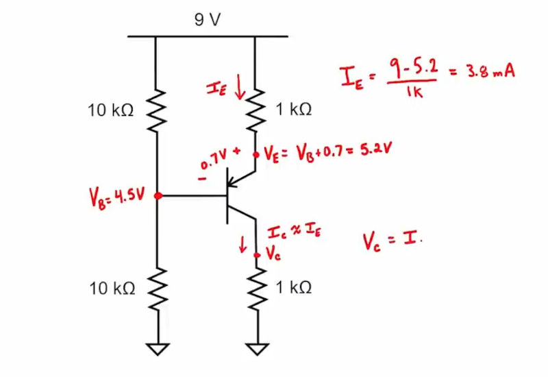
Like an NPN transistor, a PNP can operate in saturation, linear operation, reverse active, or it can be cut off. [Aaron] shows you how to bias a transistor and you’ll see it isn’t much different from an NPN except the base-emitter diode junction is reversed.
As you might expect, current has to flow through that diode junction to turn the transistor on. The arrow points in the direction of the diode junction. If you want a refresher on transistor biasing, we got you. Sure, you don’t need to do it every day now, but it still is a useful skill to have.


NPN silicon transistors are more common simply because they are easier to manufacture, and therefore cheaper. With early germanium transistors, most devices were PNP for the same reason.
Nope, it’s because of superior carrier mobility in N-type semiconductor compared to P-type. NPN is just better – faster, better beta, better operational frequency. PNP were easier to manufacture back in the days though (as substrate needed to be P type, easier to dope P in bulk, I guess), so previous era was era of PNP (and PMOS) transistors.
Floyd has a textbook, “Electronic Devices: Electron Flow Version” which flips your world on its head and is pretty interesting. I thought he had an electron flow version of his “Electronics Fundamentals” text but I don’t see it in a search and my books are in storage (a book case full of electronics texts sampled out by book publishers – mostly teacher’s editions with all the problem answers).
I don’t know how the incorrect conventional current idea survived the age of vacuum tubes, where it was obvious the electrons get emitted by the cathode and flow toward the plate. Even in solid-state electronics, I always think of electron flow, not conventional flow. The arrow in diodes and BJTs points “into the wind” so to speak, toward where the electrons are coming from, not the direction they’re going.
“Conventional current flow” survived—and does so to this day—for one extremely simple reason:
that is what is taught—and has been since ‘day one’—by all electrical engineering schools as well as all physics disciplines.
It may be instructive to understand why the arrows in diodes, BJTs, MOS transistors, UJTs, et al, ‘point’ the way they do—these representations were created by physicists and classically-trained electrical engineers.
What I don’t know, and cannot comprehend at all, is why that sub-set of the Electrical Engineering educational system (‘Electronics Technology’—for the training of people whose job is to assist Electrical Engineers ) felt it necessary to unnecessarily complicate a very-well-established subject and pedagogy by arbitrarily (and capriciously?) dictating the teaching of “electron-current-flow”.
Yes–the two are absolutely equivalent (just change the signs in your arithmetic).
No–the artificial complication is NOT needed. It is completely unnecessary and needlessly confusing to the tech school graduate once he / she gets a job.
Don’t think of a diode symbol as an arrow, showing conventional current.
Rather, think of it as (negatively charged) plate – that is spraying electrons toward a positive target.
You should all try using NNN transistors to save on P.
It is the only way to save the planet!
Isn’t that a FinFET?
Great subject; great video.
To reiterate what you’ve already said, PNP transistors are absolutely essential for switching a positive supply to a load; like, for example, a grounded LED (or a grounded ‘anything’) replacing the 1K collector resistor in the opening diagram (“…for example, when you want to switch a voltage instead of a ground…”), and for building transformer-less complementary-symmetry audio output stages (“…There are also certain amplifier configurations that need PNP units…”).
Even though hardware designers—and hardware design— seem to be in the minority these days, articles like this are still very much needed.
Thanks.
Sort of, you can also get into the quasi complementary configuration, with all n devices. The problem with complimentary outputs is while they look nice on paper, the P devices are a lot slower, so either you have an amp that has an asymmetrical slew rate, or you add capacitance to be base of the n devices to make them as slow as the P devices are. Just cause the schematic looks pretty and symmetrical does not mean that it operates that way.
If we can make H-bridges using only n-channel MOSFETs, I’m pretty sure we could use an NPN transistor to switch positive load. Using PNP may be the easiest way but I wouldn’t call them essential.
Hmmmmm… The schematic and calculation notes assume because there’s a voltage divider of 2 (x) 10 k ohm resistors that the voltage is 4.5 volts at the center junction and totally ignores the base emitter current through the lower resistor. To properly understand the voltages, particularly with the resistance values shown, you have to consider the additional current into the base junction and know the hFe of the transistor being used.
“Beta times the Base current equals the Collector current.”
-A tech school mantra
In transistor circuit analysis, it’s been common for a very long time to ignore any contribution (or effects) due to base current because of the very high beta of most transistors.
Of course, it’s still your responsibility as the circuit designer, to make certain that this can be done; that the base current contribution to the external circuit(s) can be ignored.
He did that. Watch the whole video. The base current is neglible.
He did go over that. I think in one of the examples, and I think it was in one of the flawed ones, where the base current was a factor, but the emitter voltage and the collector voltage added up to more than the supply voltage. In the next couple of videos he also makes some assumptions about caps having no resistance but delving into the “little” e emitter resistance. The delving was interesting but when the value is really low, unless you know the reactance of cap values at different frequencies in your head, and I don’t, though probably should, it is worth looking at it, because that may well be the dominating factor. I plan on going back for more. I like his style, though 3 in a row was about all I can deal with.
i like when i can use small signal transistors and pretend that a pn2222 and pn2907 are exact mirror images of eachother (nevermind that someone dumped a jimpak 50 set of 2n4401s into my ‘2222’ drawer). the moment i start building a power anything, i get frustrated by the immense number of trade offs possible, and the fact that there’s not automatically a PNP and NPN that are equivalent for a given trade-off. i get the same frustration with FET transistors…i want “a generic small signal FET” but there are so many trade offs to consider. i feel like in some ways we were luckier 20 years ago or 50 years ago where the limitation of “what i can buy at radioshack” made so many decisions for you.
the only reason i can wade through any of this stuff at all is that at prototype counts, the only difference between a $2 transistor and a $0.02 transistor is shipping time! if i had to tune a design for mass manufacturing i’d have to learn so much more :)
You don’t have a bucket of 2907 and one of 2906?
Way back in the day I designed an audio power amp that was way ahead of it’s time. IR had just released it’s hexfets, and I was raring to use them. It was a quad op amp, one of the three was current boosted for the audio, two watched rail currents, averaged a bit, and if they got too high, pulled the plug and the last one tracked a thermistor on the heat sink and if it got too hot did the same, even though they claimed the hexfets were not prone to thermal run away. Neat gadgets, good specs, relatively indestructible.. Only I had not fully anticipated the cost of the P channel hexfets. Hell, they were giving the n channel ones away if you wanted to play with them. I almost coughed up a lung when the p channel ones were like $60 a pop in single tube quantities. They gave me a couple to play with but I was really counting on a lower cost. Oddly even today, like 40 years later the P ones are still real pricy, and slow, though the p vs n thing was not apparent to me at that age outside of the cost. As a younger person, negative feedback fixed everything.
In industrial electronics and PLCs, the outputs are still referred to as NPN and PNP. NPN switches the output to ground and PNP switches the output to positive voltage. I always thought it was a pity they didn’t keep up with the jargon and started calling them “high side” and “low side” like with MOSFETs. Might have saved a few headaches. (NB I’m not an industrial engineer. Perhaps someone can provide more information)