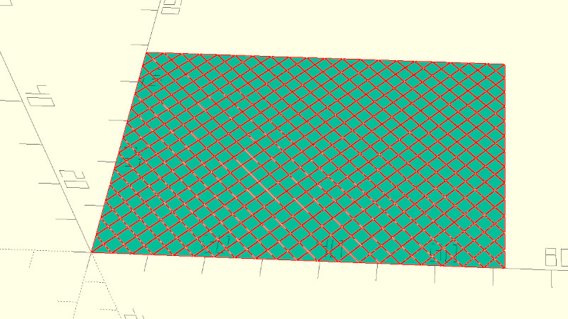
Many of us use touch pads daily on our laptops, but rarely do we give much thought about what they really do. In fact they are a PCB matrix of conductive pads, with a controller chip addressing it and sensing the area of contact. Such a complex and repetitive pattern can be annoying to create by hand in an EDA package, so [Timonsku] has written a script to take away the work.
It starts with an OpenSCAD script (originally written by Texas Instruments, and released as open source) that creates a diamond grid, which can be edited to the required dimensions and resolution. This is then exported as a DXF file, and the magic begins in a Python script. After adjustment of variables to suit, it finishes with an Eagle-compatible board file which should be importable into other EDA packages.
We’ve never made a touchpad ourselves, but having dome other such repetitive PCB tasks we feel the pain of anyone who has. Looking at this project we’re struck by the thought that its approach could be adapted for other uses, so it’s one to file away for later.
This isn’t the first home-made touchpad project we’ve brought you.


The key takeaway from this is that the Eagle board file is just a text file, and the geometry description for the elements is in a pretty straightforward format. It’s easy to generate arbitrary shapes and layouts with simple scripting, cut&paste, export from a spreadsheet, or even just manually typing it in your favorite text editor.
It’s good to start with the board file generated with all the other components first, with a placeholder part where you want the final pattern: replace the text describing that part with your text.
hahah my first thought on seeing the headline is that this is a great strength of openscad and if only they could import openscad output into kicad or whatever. but now that i’ve read your comment yeah i would have skipped openscad and gone straight to ten lines of perl :)
Pretty much all industrial/production file formats are text files, starting with famous DWG. Binary document formats are non-portable and evil
*DXF. DWG is proprietary environment.
Eagle? Ugh. KiCad please
A quote from the GitHub repo:
You can easily do thus in Altium with your eyes closed. No need for any external input. Just good knowledge of the tool. Get a better EDA!
But you didn’t need to, it’s not hard with a text editor of your choice, let alone any package capable of generating the right data, down to a few lines of any scripting language. Altium isn’t necessary at any point in this process.
It’s a great piece of software, but claiming it’s easier just means you don’t know how to do this sort of thing.
First see the bank to get a loan :(
Maybe we’ll get a built-in touchpad on this year’s Supercon Badge?? :)
Maybe the year after! This year is going a different direction so far.