
Printed circuit boards were once so simple. One or two layers of copper etched on a rectangular fiberglass substrate, with a few holes drilled in key locations so components could be soldered into place. They were functional objects, nothing more—built only for the sake of the circuit itself.
Fast forward to today, and so much has changed. Boards sprout so many layers, often more than 10, and all kinds of fancy geometric features for purposes both practical and pretty. But what catches they eye more than that, other than rich, saturated color? [Joseph Long] came to the 2024 Hackaday Supercon to educate us on the new world of full color PCBs.
[Joseph] begins his talk with an explanation of terminology. We often look at a PCB and cite its color—say, green for example. As [Joseph] explains, the color comes from the solder mask layer—so called for its job in ensuring solder can only go where it’s supposed to go. The solder mask sits atop the copper layer, but beneath the silk screen which has all the component outlines and part labels.
Solder mask was traditionally green, and this is still the most common color you’ll find in the majority of electronics. However, in recent decades, the available gamut of colors has increased. Now, you can routinely order yellow, blue, purple, and red solder masks quite easily, as well as black or white if you’re so inclined. As some creative makers have found, when designing a board, it’s possible to get several colors into a design even if you’re just using one color of solder mask. That’s because the solder mask appears in slightly different shades when it’s laid over the bare fiberglass of the PCB, versus being laid over copper, for example. Add in white silkscreen and you’ve got quite a lot to work with.
PCB Color Palette
byu/Half_Slab_Conspiracy inPrintedCircuitBoard
Different colors are achievable on a PCB even just by using a single soldermask color.

But what if you want more? What if you want real color? [Joseph] realized this could be possible when he found out that PCB board houses were already using inkjet-like printers to lay down silkscreen layers on small-run boards. Since there was already a printer involved in the board production process, wouldn’t it be simple to start printing on circuit boards in full color?
As it turns out, this was very practical. Two big Shenzhen board houses—JLCPCB and PCBWay—both started delivering color printed boards in 2024. The method involved using a white solder mask layer, with a full-color “silkscreen” layer printed on top using UV-cured ink. Using this ink was a particular key to unlocking full color PCBs. The UV-cured inks are more robust under the tough conditions PCBs face, such as the high temperatures during reflow or hand soldering.
Color printing PCBs might sound trivial and only relevant for cosmetic purposes, but [Joseph] points out it has lots of practical applications too. You can easily color code pinouts and traces right on the the board, a feature that has obvious engineering value. You can even use photorealistic footprints to indicate where other board-level modules should be soldered in, too, making assembly more intuitive. Plus, full color boards are fun—don’t discount that!
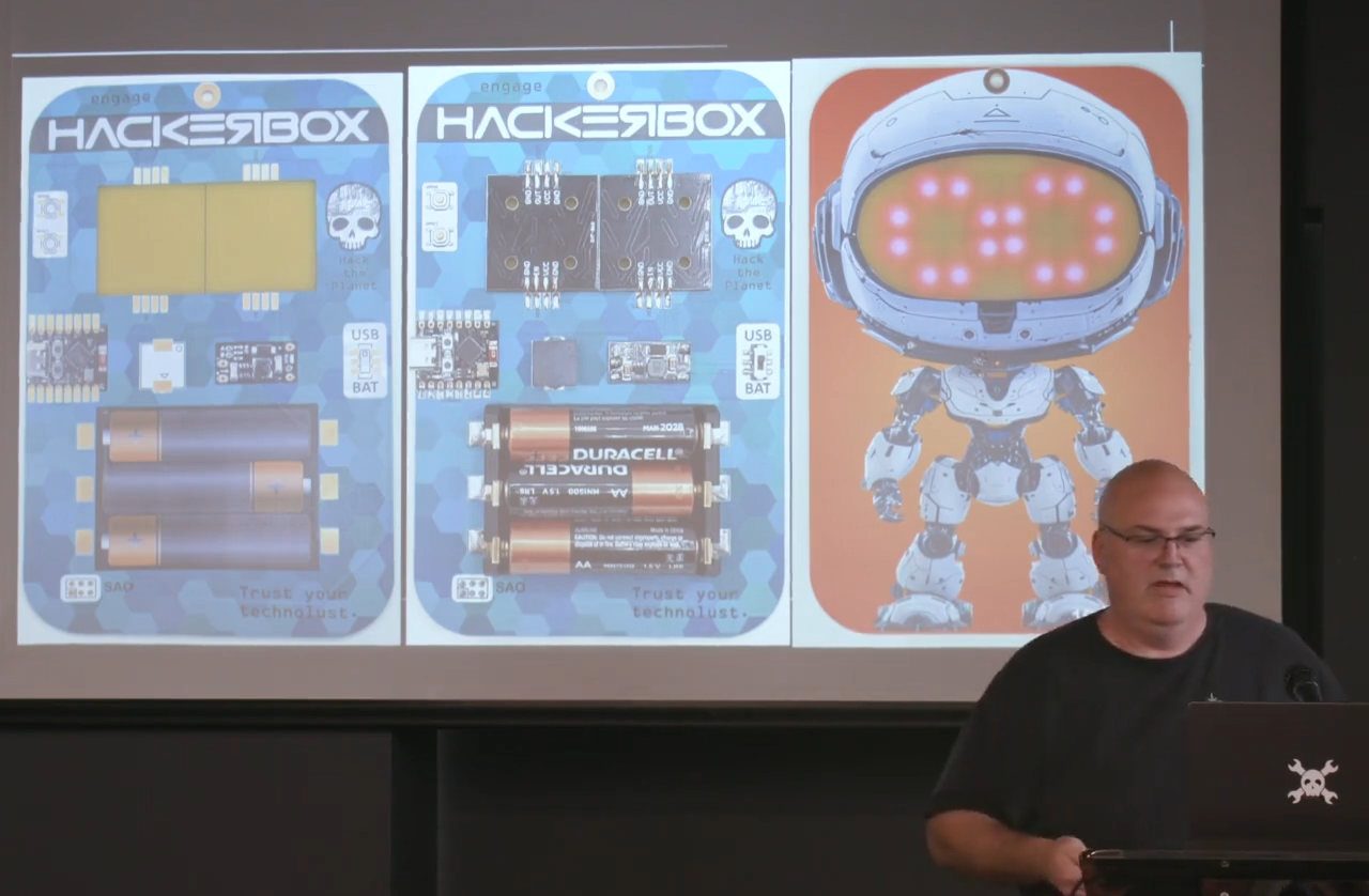
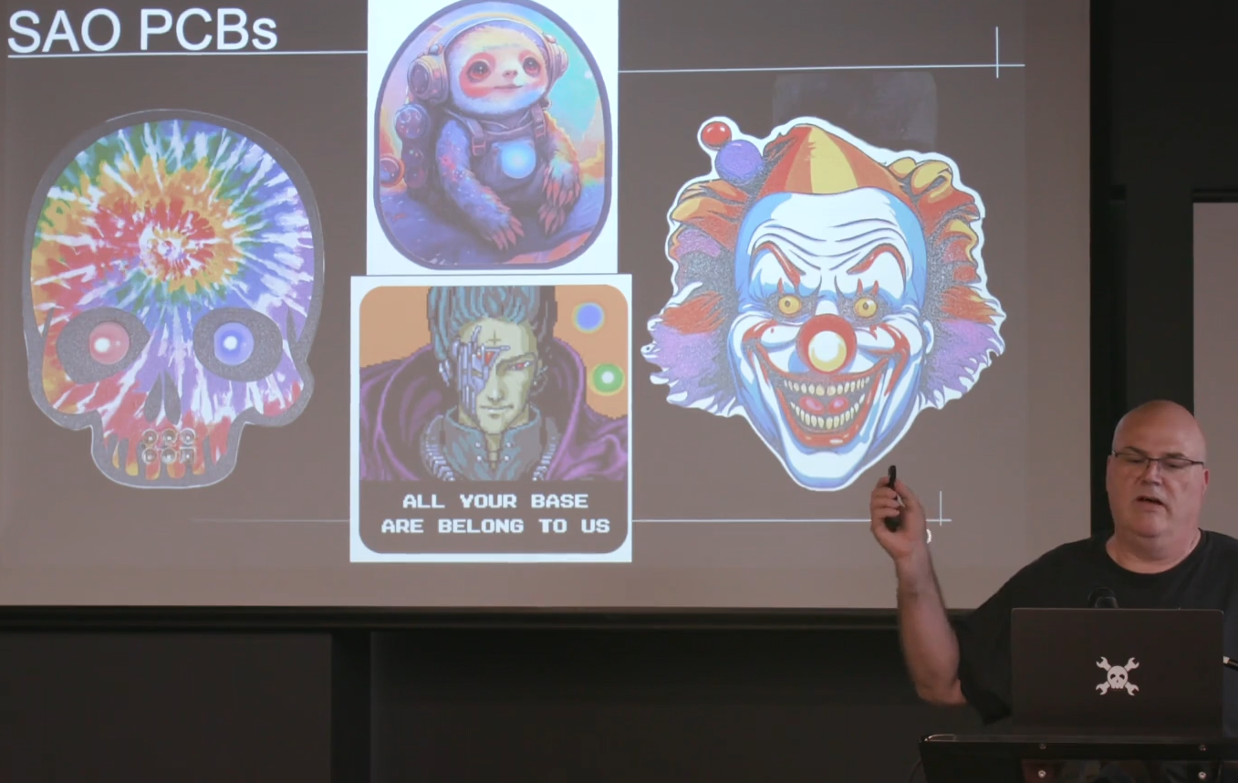
As a bonus, we even get to see some of Joseph’s awesome color boards. The graphics are stunning—they really show the potential of full-color PCBs and how they can elevate a project or a fun badge design. If you’re eager to try this out, go ahead and watch [Joseph]’s primer and dive in for yourself!


Except that it’s art, which means maybe it doesn’t go obsolete..
No functionality means no parts, most likely, in which case it’s not exactly “e”. You could call it “waste” if you don’t care about its intended lifespan as an art piece, but then you could probably do better by fighting the action figure industry than a much more niche market.
Yeah, I’m going to have to do this. I was also reacting to the “you have to use our software” thing, but if it can import from KiCad, all I would really have to do in their software is the UV-printed layers.
It s a wonderful art until seing components price and other stuff required to attach its
Funny. I can remember seeing some colored print work where same color wires were attached. Also some simple outline shapes of daughter boards or metal casings where RF bits were mounted. Things like the holes for access to tuning slugs might be depicted as circles within the boundaries of the shield box art. I figured the few boards with colors, other than only green, were intended as something of an identifier.
Outlines of TO-3 or TO-220 case were often seen
These were probably (primarily) Japanese(?) sourced boards with some secondary work done on the “Americas Continents” , based on the era and the many “Through-Hole” components still in use.
The lettering was mostly in English.
Was interesting to see a board with colors abbreviated in two or three languages sometimes. The locations of the language was what made me think that the broads traveled to different countries an perhaps different end user markets?
So I just figured the colors and outlines were an effort to reduce board stuffing errors.
Was a bit like reading the multi-lingual instructions for our gadgets and hoping to learn a bit of the lingo around “Do Not Immerse IN Water!” and “No User Serviceable Components Inside” in other languages. ;)
Anyone else remember all of the various colors of lacquer(?) dabbed onto screw heads in the Japanese electronics, in the 60’s & 70’s? Those gorgeous, Yellow Zinc plated chassis ?
Oh i just did a drone PCB and prototype . it cost around 200$ dollar from buying solder and components. And a several months to program and release it as application software . at begin , i want it become open source to drown drone price , however i realize it s not that simple. To decrease a price it required a logistic chain ,supported with reusable firmware, and strongly support by producer. I think a beginer shouldnt taste PCB unless they have a full support from supplier.
For anyone curious, 200 dollar in my country around 2/3 month salary. And even using local supplier it still too costly.
Dev on developed also not gain any profit, it only have a small profit when doing project base on scale , and negotiation . but it have a trade off between technology knowledge and society knowledge.
So basically, to make a PCB color available to nomal people, it needed a functionality of PCB give to them . and i think it s about the price not about color .
Or signage. PCBs are pretty tough stuff. So if you need a picture that lasts in a challenging environment it might work.
After watching the above, one thing doesn’t make sense to me. When preparing the color image to be printed, we have to find all places where there are holes or exposed copper, and make those areas transparent in the graphics file.
Doesn’t the fabrication house know where the wholes are?
Can’t they calculate where the transparency should be in the image file?
Yah the fabrication happens before the “silkscreening” in this case, and the two manufacturers do different processing. PCBWay prints at the end, like an inkjet printer, so you need to keep your pads cleared in your design. The video explains this a bit more.
MCUs and PCBs aren’t just toys. The controller in your furnace thermostat, the computer in your microwave oven, the computer in your dishwasher, the computer in your air fryer are all MCUs on PCBs. All of these commercial products started out life as modular breakout boards that allowed design reconfiguration as the product was developed.