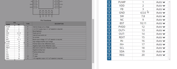
One of the big problems with doing PCB layout is finding a suitable footprint for the components you want to use. Most tools have some library although — of course — some are better than others. You can often get by with using some generic footprint, too. That’s not handy for schematic layout, though, because you’ll have to remember what pin goes where. But if you can’t find what you are looking for SnapEDA is an interesting source of components available for many different layout tools. What really caught our eye though was a relatively new service they have that uses computer vision and OCR to generate schematic symbols directly from a data sheet. You can see it work in the video below.
The service seems to be tied to parts the database already knows about. and has a known footprint available. As you’ll see in the video, it will dig up the datasheet and let you select the pin table inside. The system does OCR on that part of the datasheet, lets you modify the result, and add anything that it missed.


