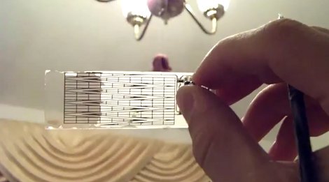
Our friend [Jeri] tipped us off about this cool video on youtube where the author makes his own “transparent” PCB’s using some nontraditional materials. One ounce copper foil is found online along with some clear glass microscope slides, from there it is just a matter of cementing the foil onto the glass slides with some thin UV curing glue. Once the 2 parts are mated the entire thing is popped into an eeprom eraser for its intense UV light, then excess is trimmed.
The normal routine of toner transfer is used to copy a circuit pattern onto the copper clad glass and it’s etched in standard ferric chloride. The copper is removed but the UV glue that was holding it is still left, some special care needs be followed as this stuff is pretty weak against even mild solvents, and you do not want your traces peeling up. Next no clean solder paste is applied and parts are soldered down with a heat gun, keeping the glass evenly heated to prevent it from cracking.
This leaves you with a board that looks like frosted glass, and in order to protect the glue while clearing up the frosted effect, some polyurethane is applied which fills in all the little bumps and smoothes the surface bout out to almost 100% clear.
The end application in this video is a touch sensitive board which works fine though the back side of the glass and presents a nice smooth interface for the user. Join us after the break for the video.
[youtube=http://www.youtube.com/watch?v=Rf5HBLzDGQA&feature=mfu_in_order&list=UL&w=450]


Ahh, when making a PCB is not hard enough, adding glass to the mixture.
Tomorrow on HAD, making your own PCB’s out of thermite and black powder…..
c’mon man, I almost snarfed yogurt. :)
I nearly choked as well.
Haha That really got me. I am still smiling like a mad man. :)
“This device will now self-destruct.”
Neat, very thorough.
What a sink!
Common in old houses, huge & made from concrete or similar.
You needed a big sink to wash your clothes before washing machines were invented.
OT, you can get adhesive backed copper foil (used for shielding etc), but after etching you’re left with the adhesive. I did try it years ago, wasn’t really happy with the result.
I could not find any adhesives that would survive the hot air process. Do you have a link?
You can get copper tape for making stained glass, the adhesive doesn’t survive soldering for that long, it only comes in thin strips.
The 3M shielding tape is this stuff: http://www.l-com.com/productfamily.aspx?id=1921, probably exactly the same adhesive but at least it comes in 1″ thicknesses, just right for slides.
I have seen similar sold to wrap around plants to ward of snail & slugs.
Of course there’s high temp epoxy, but application could be a hassle.
I’m idly wondering if I could powdercoat copper foil, place the slide on top and cure it, bonding the two together. Powdercoat cures at 200C (~400F), but handles nearly twice that once cured. Hmm.
I just placed an order for some 1″ 3M tape.
Actually it’s my parent’s sink, and I’d pay some $$ to get one in my house. Concrete sinks are the best.
that’s cool, you gotta love it!
well it LOOKS pretty. be nice to see a glass motherboard if thats even possible (i didnt even know you could USE glass…so…) all glass computer would look pretty and break REALLY easy…maybe make it a mac.
Well, of course you can use glass. You probably already are using glass and resin for circuit boards, this just takes out the resin. (Circuit boards typically are various types of fiberglass)
i always thought circuit boards were made from silicon wafers
you know it kinda looks like an isolinear chip from star trek (TNG+) perhaps someone could add some embedded memory.
@austin
Integrated Circuits are made of silicon wafers, but circuit boards are made of various materials. It’s rare to see large silicon-based stuff, since the crystals are fairly expensive to grow. You can’t just use molten glass, since it won’t properly form transistors.
This process is currently limited to single layer boards, but lucky me, I left the world of two-layer ages ago.
I wounder if this can be done to a LCD to make it a touchscreen. Either way this is cool.
As far as i can tell aside from having to use hot air reflow, the biggest annoyance with this would be drilling holes for vias, if you wanted to do double sided pcbs. But on the other hand a multilayer glass pcbs (without ground and vcc planes) would look pretty cool.
To avoid problems with drilling holes in glass (although apparently it’s possible) maybe run the traces to the edge of the glass to the other side and join with thin wire?
The copper leaf looks thin enough that you could probably use a simple bookbinding method of folding the leaf around the slide like you do with the covers of books.
There would probably be a small gap on the opposite side but then you can just use a small jumper like you normally would.
Very nice indeed.
How about all single-sided boards, and connect them by one other singe-sided glass board? Like a mainboard and expansion cards, but now fully transparent.
You could etch the holes into the glass, but hydrofluoric acid is really nasty and toxic stuff.
On the other hand THEN the full PPE and tyvec suit would be adequate. When I etched my PCBs I just used old clothes and opened the window as the fumes from the HCl/H2O2/H2O mixture were quite unpleasant. Although a few second of exposure of the skin to the mixture were no problem, I normally just took out the finished PCB with bare fingers.
I’m wondering what would happen to the slide as it rolls through my laminator. Cool, but maybe I’ll stick to pc board material.
That’s what really surprised me – it survives the lamination AND ironing process without any problems.
I wonder if process similar to silvering mirrors could be applied here to avoid using adhesives.
That’s the method most commonly used to make intricate boards – rather than etching away material, its electrically built up in the pattern wanted. Trick would be to find a resist for that first tin layer.
I suggest the use of bicomponent epoxy… it is usually temperature compliant with soldering too and it don’t dissolve easily in any solvent. Of course it cure in more time.
Really great pirce Kevin! I love the idea of etching on glass. And your use of FeCl was very well done.. with nice results. :)
Have you had any problems with the fragility of the glass being used as a board? What about mounting considerations (mount with hot glue, or traditional standoffs)?
Tweeks
The biggest thing for me in the video is when he used the thing as a touch sensor. I thought it was some sort of areal until he started using it. Can anyone point to more info on that type of touch sensor?
I recently posted the source code, etc. on the main youtube article. I based my touch designs partially off of this guy’s http://www.youtube.com/watch?v=b71Vkq8dyf8 … except that the way I use it, I only need one GPIO pin. Feel free to contact me on youtube for more information. I do not check hackaday posts often.
Now do it for through-hole…. :)
Nope. I haven’t done thru hole or double layer in forever. Everything I have needed to do fits on one side. <3 SMT.
Truly, he is a wizard.
Good thorough presentation. I like that you can take it in an “artsy” direction by stacking boards, lighting effects, etc. or just take advantage of the practical aspects of an easy to clean touch surface that won’t scratch easily.
couldn’t you do a similar task with silver nitrate and some kind of a masking element like wax? I would assume that you would get better results and could have finer details on your pcb since its a somewhat gentle process when the nitrate is bonding to the glass. still a cool effect. I’d like to see this put together with Jeri’s EL hack.
I’m unfortunately a fan of “good enough” … so, once I got my process going, I didn’t really feel compelled to change it. Additionally, I’d love to see where others take this (if they do at all). I have a very specific thing I needed this for which I hope will make hackaday when it’s done.
Hm, they used to use silver nitrate in photographic film. When light hits it, it breaks down into metallic silver, which is the “dark” in the photograph.I wonder if there’s a way of using the silver as conductive tracks? The first photographs were on glass plates. Perhaps just use a thick layer of the silver nitrate? Perhaps connect the silver layer to a power supply, dip it in a tank, and electroplate it with copper?
It might not work, but it’d be interesting to see. A PCB that’s literally a photograph! Easy to develop using normal light in a dark room with maybe a red bulb.
They used silverbromide and -iodide – which can be made out of silver nitrate. There is also a PCB printer using a silver salt (nitrate?) and citric acid as a reducing agent in an inkjet like process. But its always the problem of plated vias. Even as I use SMD I often needed multilayer or at least double sided PCBs, often with componets on both sides.
glass naturally attenuated UV….
Attenuate – yes, but not completely and the used microscope slide is very thin.
The plural of LCD is *not* “LCD’s”!
yes it is.
No, “LCD’s” is the possessive of “LCD”. The plural is “LCDs”
It’s actually a regional thing. Apostrophe+s is a completely valid alternative way to pluralize acronyms in a good part of the world.
Epoxy might work, although most types have a yellowish tint.
I was thinking about this, and wondered if the porous Al hack Jeri came up with would allow a “glass” EL sheet to be made if 1/4 of the panel was porous Al and 3/4 was Cu.
To get a grid display you would need to do a photoetching step before the porous step and electroplate off the Al where the grid divisions are to be.
This is well beyond my skill set – but if you are someone who’s equipped to play with EL then I think anything further with hobbyist EL would be awesome.
I’m envisioning a mp3 player with this capacitance touch method for the interface. Would it still work through plexiglass? I wonder what ferric chloride would do to plexiglass…
I’m dumb.. plexiglass would melt wile soldering. I should really think things through before I comment…
Polyester copperclad stock (thin and flexible though) is available eg from Farnell, and is solderable though you have to use a real temp controlled iron and leaded solder and be very careful.
This is normally Polimide which is much more heat resistant. Th FeCl3 would do nothing to the plexiglass and you could use low temp solder, like the chipquik stuff (melting point about 60°C) or conductive epoxy for the arts, if you want
Lead-free solder has a lower melting point.
Thats why PS3s and XBOX360s fall apart when placed on their sides.
Wow, that’s the most incorrect thing about soldering I have seen on this site. Lead-free solder has much higher melting point than leaded solder.
Console failures occur due to poor cooling. Repeated heating and cooling of chips cause stress and cracks in brittle lead-free solder. Leaded solder, being much softer, would survive this much better.
Ooo,, this gives me another stupid idea. Do you think that copper leaf could be run through a printer itself? Maybe we could remove the “transfer” part of the toner transfer method.
BRILLIANT!!! I think I will try this! It would make it possible to adhere to much thicker sheets of glass! I never considered it!
Have a lok at this: http://www.pbase.com/mark10970/direct_laser_pcbs
I didn’t this was actually possible, I thought the copper would be too conductive and screw things up. If that works, then a ‘copper on glass’ PCB would. You won’t get 2-3mm glass thru a laser easily though.
Toner based printing uses static electricity to attract the powder to the paper, that would not work using metal, though you could use a thermal transfer printer (ie label printer).
Lame… I just gutted and tossed a datamax thermal transfer printer a couple of months ago after my failed attempt to get some FR4 board to go through it…
Actually, laser printers and copiers use electrostatic charge to attract toner to a transfer drum (or belt in some cases) which is pressed against the paper. I’ve successfully printed on conductive materials (including aluminized mylar) with a LaserJet.
Make yourself a favour and dump the toner idea alltogether – Epson yellow ink is FeCl resistant and you can print boards using CD printing ability without modifying your printer. Now you can make round 120mm boards. Or fill your inkjet with conductive ink and go for electroplating.
How about using a front silvered mirror as a PCB? It’s already a bonded coating, and can be etched and soldered. It probably needs to be plated thicker, but it should work great.
I spent about a month going down this road, but angel gilded copper is far too weak to stand up to ANY kind of soldering process and can’t really be electroplated… And we had difficulty copper plating the aluminum to be thick enough and even.
Too many ‘e’s there, you said “eeprom” which is “Electronically Erasable Programmable Read Only Memory” You meant “eprom” which is “Erasable Programmable Read Only Memory” eeproms don’t need UV light, eproms do. :)
UV laser cnc anyone?
Very VERY COOL, imagine a whole window with that awesome diamond pattern on it controlling something like an LED table, or the blinds…….
has it occurred to anyone that the usefulness of this creation may be it’s fragility? Top Secret hacks can be destroyed easily, quickly and effectively if your pcb is made of glass. Amirite?
My first question was how do you drill the holes in the PCB without breaking or cracking the glass.
I see the answer is not to drill any holes.
Maybe you can use a transparent sheet of plastic. Then solder very quickly not to melt it.
Sure you can drill holes in glass. You only need very powerful fast pulse laser. Or waterjet. Or sharp drill (broken needle file works good) and lots of coolant.
Could you pleasepleaseplease,put the schematic up?I would love to make one of these.I am beginning to make my own circuit boards and am very good with electronics,while I have not documented any of my builds,I have made several things from scratch and this would be quite cool.
https://cnlohr.net/pubsvn/electrical/Touch/Touch5/
this link is broken
Ok! thank you!
Now I only imagine a Zaphire substrate gold leaf(aqua regia etched) pcb for some really expensive and gorgeous computer
may i know how to make the resistive ink “chemical mix that could be used as a connection wire over thin paper or plastic paper and could be soldered to smd components ”
it would be very helpful if i got my answer
another question plz !??
in PCB … is there a link for completely home made PCB tools ….and manufacturing in my small lab…..please notify
I’m not entirely sure what you’re referring to, I’ve used these pens before, and they do work, albeit not all that great…
http://www.ebay.com/itm/NEW-Caig-CW100P-CONDUCTIVE-TRACE-PEN-Circuit-WRITER-PAD-defog-USA-Made-bus-fix-/300751516436?pt=LH_DefaultDomain_0&hash=item46062ff314
I would say that this process is completely home made, it only takes about $200 worth of equipment (plus a laser printer)
hi, can you please tell me about the programmer of the ic used in this project, and components value.