The lowly diode, a device with only two leads, can nonetheless do many things. Diodes can detect, rectify, suppress, emit light, detect light, change capacitance, emit microwaves and more. This wide range of use means diodes are included in almost every design and it’s well worth learning more about the inner workings of all kinds of diodes.
My introduction to diodes started like many of my generation with a homemade crystal radio set. My first diode was a piece of pencil graphite in contact with an old fashion safety razor with the joint of the two dissimilar materials — graphite and steel — creating the diode. In this configuration the diode is said to be “detecting” which is the act of turning a weak radio signal into a weak audio signal. At least in my home town of Marion Indiana, one radio station was stronger than the other so that I didn’t have to listen to two stations at once.
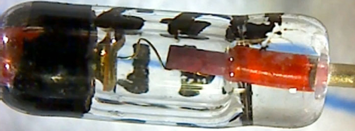
I eventually learned about “real” diodes and the 1N34A Germanium diode was my “goto” diode into my teens. Nowadays looking into a modern version of the 1N34A you can still see the semblance of the old “cat’s whisker” by looking carefully into the diode.
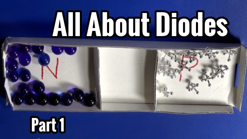
A quick and somewhat inaccurate semblance of the way a diode works can be demonstrated with marbles and jacks representing negative electrons and positive “holes”. Holes are basically an atom missing an electron due to the combination of elements, a process known as doping. Join me after the break for the explanation.
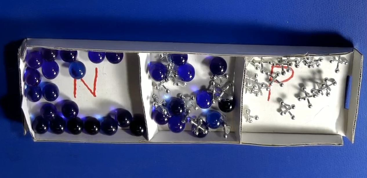
At rest some of the electrons and holes combine to produce an electrically neutral atom that acts as an insulator since electrons cannot readily jump to and from the atom now that it’s locked up.
If we apply a voltage in a reverse direction, holes and electrons pull away from the center and no current flows, the central zone, known as the depletion zone, gets larger. Connecting a voltage in a way that makes more electrons, (more “potential”) available to the N material starts to push electrons across neutral barrier a process known as breakdown. In the video I show the electrons (marbles) pushing the depletion off one end, in real life there is a crystal lattice and holes are flowing in one direction while electrons are flowing in the other, the goal was to show a simple difference about why a reverse connected diode works different that a forward biased diode.
Schottky and Zener Diodes
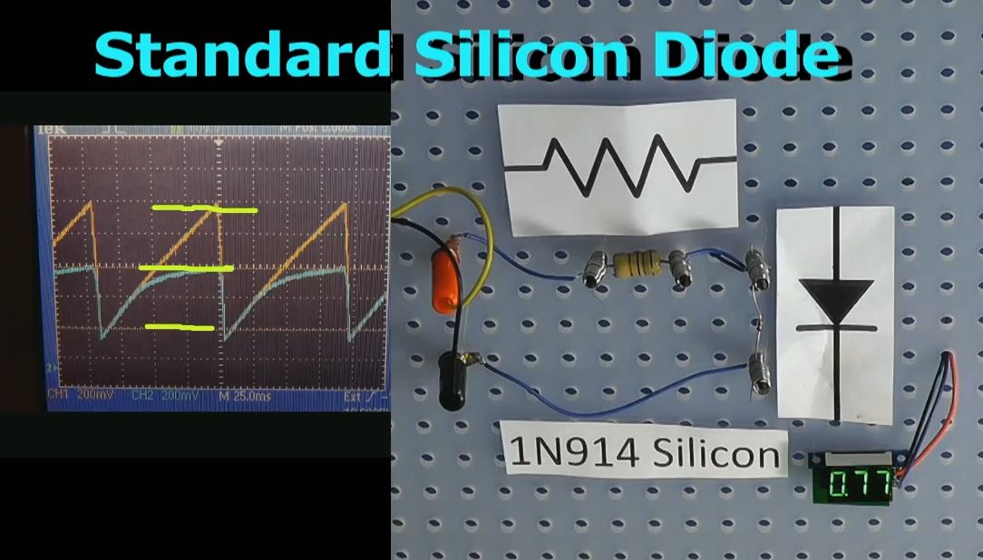
Schottky Diodes are available that offer a lower Forward Voltage Drop than silicon which also means less power dissipation. As a quick visual of the difference between a silicon diode and a Schottky diode we subjected the devices to a 1 volt ramp signal and visually demonstrate the differences as shown below.
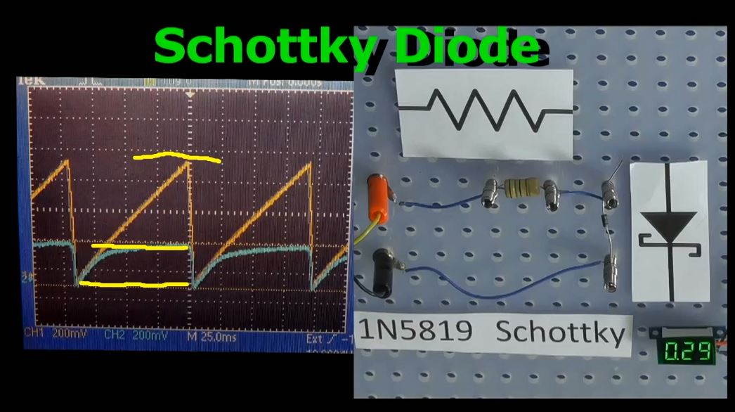
It should be noted that this isn’t a common way to use these devices, this was mostly to show the proportion of a 1 volt signal that the diode selection can affect. In the older days we mostly saw Schottky in RF applications as the low capacitance and fast recovery time worked well at high frequencies.
Another piece of information that I picked up while young was that a good number of Zener Diodes were not really true Zener Diodes they were in fact avalanche diodes. With that said they did pretty act much like their Zener cousins and so the lack of visible differences allowed users to indiscriminately use either.
Alas, back then in the before time, there was no Internet to look up or verify facts like this, so one pretty much had to commit brains cells for storing the semi-useful facts on the off chance it would make be needed some day. Also I must admit that I was curious if I could tell the difference between the two so out came the 5 digit Keithly VOM and a heat gun.
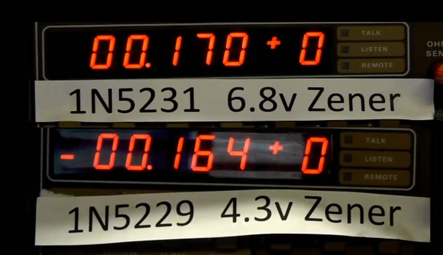
As it turns out the identification between a Zener and Avalanche diode can be ascertained by checking whether it has a positive or negative coefficient (reaction to heat). Shown are two different voltage diodes after the meter has been zeroed and the diodes heated. An interesting fact is that at around 5.6V the breakdown voltage is due to roughly half from the Zener effect and half from the Avalanche which results in the temperature characteristics tending to cancel out.
If this discussion got you thinking about the effects of temperature change, make sure you watched my video about calculating component heat.
Crude Voltage Regulation
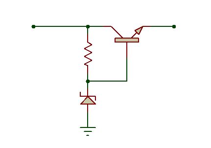
A very common voltage regulator was made back then with a power transistor in a Common Base configuration with the base voltage set by the 5.6v Zener. The circuit shown here is a somewhat crude regulator and didn’t have the kind of load regulation and other qualities we assume that we get with our 3 terminal regulators.
Whether the diode is a Zener or Avalanche (or both) isn’t real important if the part is specified correctly, with the exception that transient voltage suppression diodes tend to be Avalanche style.
Finally when working with analog circuits where the forward voltage drop is significant, an OpAmp can be used to overcome the drop while still providing a directional conduction. In this case the diode is included in a negative feedback loop where most of the undesirable effects are canceled out. Shown working here as a simple rectifier, variations of this circuit find their ways into peak and hold circuits and audio detectors.


Stopped watching after 3:00
Is this a troll video or something? WTF?!?!?!?!!!!!!!!
wtf are you on about
Excellent video Bil, thank you for making it.
What is your exact critique here…or is this a troll comment or something? ;)
I believe the issue is with the description/presentation of a diode in the forward biased mode. As far as I understand, the depletion region of a diode does not get “pushed” out of the diode. I may be wrong, but I always believed that the depletion region was compressed while the diode was forward biased.
If this is not the case, can anyone point me to a theoretical description of a varactor or varicap supporting the “pushed” depletion region behavior?
That struck me too as an odd representation.
After I shot it I thought the same thing and mentioned in the post that there really is a lattice with counter flows of holes and electrons. I was trying to show that it took a certain amount of pressure to overcome the depletion region and reverse caused bunching at the leads.
The marbles were a replacement for not having a good animation to show, and I am trying to think how to show the depletion compressing and conduction, maybe some plexiglass cut and welded would give a better model. Its definitely a continuous effort to try and find reasonable visual props. I humbly submit that one day I will post a better way of showing the forward voltage breakdown.
I spotted it :-)
on the 3min mark: “pushes the barrier down the diode” – err, yeah.
It’s all about mobile charge carriers and in all materials, electrons live at unique energy levels. When electrons can move around freely (because they’re not locked “orbiting” an atom), they’re in a higher level called the “conduction band”, the ones that are stuck are in the “valence band”. Now, to get the electrons into the conduction band, then you either need the two bands to overlap so it’s easy for electrons to promote themselves (what happens in a conductor) or there’s an excess such that they’re just sitting around there (n-type silicon). Alternatively, if you can remove of some electrons in the valence band such they could ‘shuffle’ across (think of a sliding block puzzle), where one actually sees the charge carrier being the absence of electrons, i.e. holes (p-type silicon).
When a diode is conducting, the holes and electrons are *both* moving towards the gap in the middle (where there is no majority charge-carrier) and when they reach that point they recombine because, like most physics, the electrons would rather live at a lower energy (this drop/release in energy relates to the emitted colour in LEDs… except the ones that use a phosphor). There is no “pushing” of this zone towards either end.
http://www.science-campus.com/engineering/electronics/semiconductor_theory/semiconductor_1.html
appears to be accurate.
Okay, I’ve ignored electrons being promoted by thermal means but it’s generally best to avoid that :-) (hence silicon’s resistance going down when it gets warm and why hot semiconductors are bad)
Now, the really cool effects are with diodes that don’t use a P-N junction such as Schottky diodes (they use metal and a single doped semi-conductor) and other types (which can also be metal with semi-conductor) where the electrons make use of quantum tunnelling effects (unimaginatively “tunnelling diodes”)!
And this kids, is why for all their talents, diodes will never make the olympics.
I disagree with you guys up there ^.
Even if most of the readers here are PROs there’s no reason to criticize the make of this article… I mean, you’re not paying so why to complain? If somebody have a kid or a young friend in the beginning of the study of electronics this video for sure is useful.
And, every piece of electronic is important to build things, no piece should be skipped.
I think the point they’re trying to make is that it’s important to accurately describe technology with (current) theory. It’s OK to “dumb it down” for the masses but not at the expense of changing the theory, or more importantly, the basic understanding.
To put it another way. The internet is not like a bunch of tubes and should never be explained as such.
No, the internet is a bunch of pipes and sockets… Tubes are used elsewhere.
Actually, the internet is EXACTLY like a series of tubes. Oh, the tubes are a little magical but they still obey the laws of physics. The tubes come in different sizes, and sometimes are composed of a tube wrapped in a tube that is wrapped in another tube, and sometimes the walls are squishy and soft so they collapse if things get busy… but having watched the internet grow up from the inside, I’d say that the senator had exactly the right metaphor to discuss capacity issues.
Thanks for putting together the video, for those of us without formal EE training, insight into some of the anomalies of components used every day painlessly illustrate what would take decades buried in datasheets to realize. thank you for taking the time to assist me and im sure many more.
My only critique of the video would be that you need to compress or limit the audio stream a little bit, and de-ess very harshly. In the first few minutes of the video, every S or SH or Z sound clipped on my speakers and got very harsh to listen to; so bad that I just cut the volume until halfway through.
It might just be your microphone, but I had to turn up the volume to hear you speak, and then get blown out on every ess…really painful on the ears.
It might just be your hardware too, because it sounded fine here.
cheap tablet speakers, I have to have the volume pretty high to hear the soft bits. that means that anytime the audio signal jumps from 70%~80% normal to 100%+ clipping then it’s going to crackle on these very non-linear response speakers. Hence my suggestion to compress or limit, to bring the dynamic range down.
Could be that youtube thinks I’m a full desktop and fed me higher range audio; I’m unsure of how their system works. But PCM clipping on audio is clipping, the listening hardware won’t change that. Unless you suggest youtube and my audio drivers are collaborating to boost the audio and clip; possible but I would expect to hear it on more videos.
I listened to it on a desktop with 5.1 surround sound.
I did not notice anything like that with the audio either, but I use headphones, and talking of which.. tablets have headphone ports. (and BT to stream audio).
Anyway it seems odd to complain to the maker of a video about your own faulty setup I have to agree.
Sounded fine on my cellphone, except for the very first second.
It would have been clearer if you would have mentioned what the scope was showing Orange = input signal Blue = output across the diode. Also mention where the zero line (it’s a bit hard to tell in the video). Still I found it interesting – a bit of a reminder – thanks
+1. Always define the symbols and jargon.
BTW, thanks for the video!
This is a video on the PIN diode (YET another diode!) The PIN is a very interesting diode. Understanding the intrinsic region (large depletion region) of the PIN helps illuminate how the regular PN diode depletion region works.
https://www.youtube.com/watch?v=XpYsCM_Wf50
Good lord why does nobody understand how semiconductors work!?
Okay let’s see if this can be corrected. To start lets point out a few important words.
Ones we have seen
Holes – Exactly as it sounds, a missing electron or an empty but available orbital
Electrons – Ya…
Majority Carriers – The carrier with the largest population on a side (N/P)
Minority Carriers – The carrier with the smaller population
In EE terms they are called donors and acceptors.
For example Arsenic is a donor (electron) and Boron is an acceptor (hole) so a NP diode might have Arsenic on the N side and Boron on the P side.
Now for a spherical chicken in a vacuum.
So there is a bunch of quantum physics involved dealing with valance bands, fermi levels, and Boltsmann sticks his dick everywhere but we can sorta kinda ignore most of it for high concentration dopant ratios.
There are two kinds of holes in this world. Those with electrons in them and those without. There are two kinds of electrons in the world.
A boring un-doped silicone brick will normally have some extra holes and extra electrons knocking about due to natural thermal forces such that n = p. This number of carriers is called the intrinsic carrier concentration and is very dependent on Temperature. (More on this in a bit but it is why semiconductors stop working at very high and very low temperatures).
The intrinsic carrier concentration is denoted as n_i and is equal to number of freed states.
n*p = n_i^2
The nice thing about knowing this number is, you can assume most of the nasty bits away when Nd and Na are much much larger then ni. As they are in most situations.
Okay so that’s boring as a beach. Lets add some dopants! YAAA PARTY BRO!
So after a crazy night of ill advised science you have some how managed to precisely diffuse B into one end of a silicone stick and As into the other – congratulations.
What happens now is the wonderful process of depletion! On the side with acceptors all the free thermal electrons fall into the extra holes depleting the free electrons and on the side with donors all the free holes are filled with extra electrons… almost.
So turns out there are not quite enough. In the area near where the two sides meet is the depletion region. There every electron can find a hole and vice versa. The carriers are completely depleted. As you move further away this stops being the case. Kinda like China with all those missing [CENSORED].
So what happens when you forward bias a diode.
Well basically you reduce the junction barrier height allowing for carriers to diffuse from each side to the other resulting in minority carrier injection into the episcopate side and thus conduction. Yes.
Basically basically holes are shoved into the side with holes and electrons into the side with electrons as majority carriers. When they cross from one side to the other they become minority carriers and are quickly combined with the incoming majority carriers. However since this consumes the majority carrier on that side more of that carrier can be injected and equilibrium maintained. The distance carriers can travel before being consumed is called the diffusion length.
Clear as mud?
Okay so back to the temperature thing.
If a semiconductor is too hot the number of free carriers ni will become large compared to the dopant levels. When this happens and the free carriers stop satisfying the Na, Nd >> ni rule the semiconductor stops working. Basically it cant deplete.
The other side is when it is too cold. If there are no free carriers then well nothing can move. You need free electrons on one side and holes on the other. When the temperature is very very low the natural carriers are all in combined states meaning the donors and acceptors can not deplete anything and you have no carriers to work with.
Thanks for the video. In your next one could you get a new mic? The one in the video sounds like it is damaged or being overloaded.
The “Crude Voltage Regulator” is a Common Collector aka Emitter Follower, not a Common Base configuration.
Another use for diodes: Antenna diodes. These are used in integrated circuits, but the purpose is not for circuit functionality. During wafer processing, the metallization (deposited metal layers, later etched in patterns to form the ‘wires’ connecting the transistors) can attract charge from the processing tools. With too much charge into a high impedance node, such as a MOSFET’s gate, the gate oxide can rupture and become damaged during the wafer processing. The larger the area of metal, the bigger the antenna to collect more charge.*
To prevent this, design rules and automated checkers are implemented to check how much area of metal would be connected to gates without a parallel low impedance** path to ground. Any errors are mitigated with antenna diodes, with the ‘n’ side (cathode) to the gate and the ‘p’ side (anode) to ground. (This would effectively clamp the signal to > -0.7V, but that’s typically ok for these apps.) Alternately, you could have an the anode of the diode to the gate and the cathode to VCC (or VDD), which would clamp it to VCC + 0.7V. The latter case would dissipate the charge to VCC and then through some other low impedance path to GND (ESD protection maybe?).
The part of this that is harder to describe in words is that the MOSFET gate that is susceptible to oxide rupture and the low impedance path to ground may be connected connected together in the schematic, and eventually in the integrated circuit, but what if that connection is made a higher level of metallization? Wafers are fabricated with multiple layers of metal, similar to multi layer PCBs. Anyway, the process design rules and auto checker needs to take into account the layout… it is not enough for the gate to be connected to a low impedance path on the schematic. It must be connected to a low impedance path at all times, even before that connection at the higher metal level is made at a later processing step.***
* Think definition of current = d (charge) / dt. and the voltage / current equation for a capacitor (e.g. MOSFET gate) is: i = C * dv / dt. So as charge starts collecting, you get a current on the gate, charging it up, e.g. higher voltage. With nothing to bring the voltage back down, the gate oxide will rupture.
** I’m using the term low impedance path loosely. I just mean some resistive path to ground to discharge the … charge.
*** wikipedia has a good diagram of this, google ‘antenna diode’
**** This was a lot longer than I intended.
You might also want to add these applications of the lowly diode: How to use a diode as a switch: https://www.youtube.com/watch?v=YBNIq_d56sA …and the PIN diode, a nice voltage controlled RF resistor which can also be used as a switch: https://www.youtube.com/watch?v=XpYsCM_Wf50 …and not to mention the voltage variable capacitance of the diode, including diodes specifically designed for this (varactors): https://www.youtube.com/watch?v=icw8terKP-M