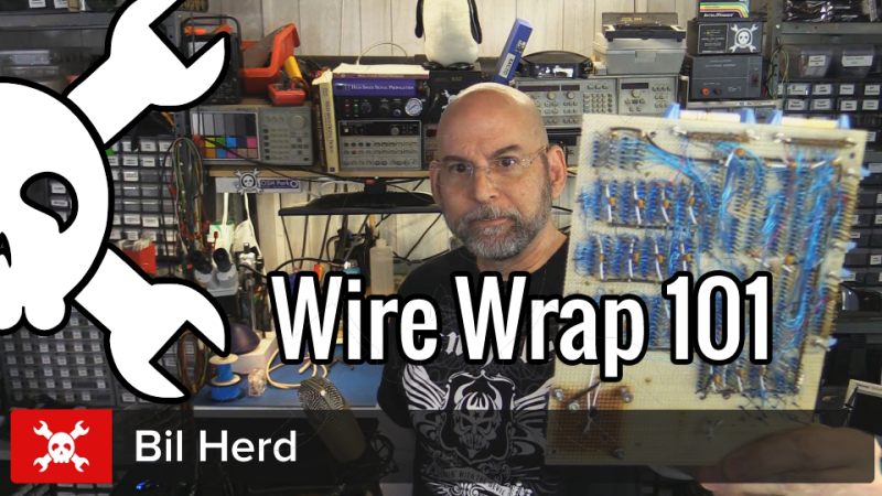
You might notice that many of my writings start with “Back in the day”. Not wanting to disappoint I will say that back in the day we used to use wire wrap technology when we needed a somewhat solid, somewhat reliably assembly. Given a readable schematic a good tech could return a working or near-working unit in a day or two depending on the completeness and accuracy of the schematic.
Properly done a wire wrap assembly is capable of fairly high speed and acceptable noise when the alternative option of creating a custom PCB would take too long or not allow enough experimentation. Wire wrap is also used in several types of production, from telco to NASA, but I am all about the engineer’s point of view on this.
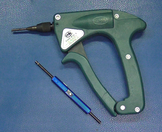
My first wire wrap tool and wire wrap wire came from Radio Shack in the mid 1970’s. I still have the wire, because frankly its kind of cheap wire and I use it when it’s the only thing I can reach quickly when I need to make a jumper on a PCB. The tool is still around also, given the fact that I can’t find it at the moment the one shown here is my new wire wrap tool which is good for low quantity wrapping, unwrapping and stripping.
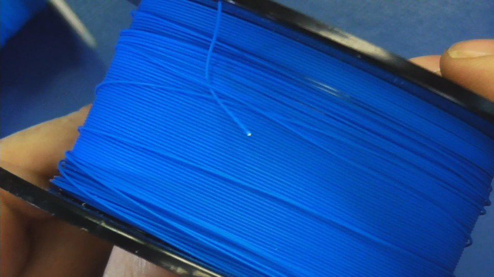
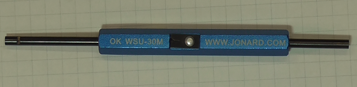 The skinny little wrap tool is okay for hobbyist as the wraps are fine with a little practice. But I do recommend investing in high-quality wire. A common wire available is Kynar® coated, a fluorinated vinyl that performs well as an insulator.
Before I go too much further, here’s the video walkthrough of wire wrap, its uses, and several demonstration. But make sure you also join me after the break where I cover the rest of the information you need to start on the road to wire wrap master.
Another important You will also hear me harp on good power and ground layout; “stubs or lengths of power supply wire that terminate in dead ends should be kept to a minimum and the power and ground wires are routed in close proximity to each other. 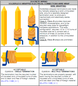 Inductively coupling the supply and return together reduces impedance, hence noise. Obviously there is a lot more to it than that but that’s for another video.
A good wrap has 3-4 turns of the exposed wire on the square post and a turn of insulated wire which improves resistance to vibration and vibration based failure. The drawing here is from the NASA standards part of their website showing an acceptable wrap.


Wire wrap sockets are still available and I keep wire wrap SIP terminal strips as a custom socket footprint can be created as needed.
For more complex wire wrap components such as connectors you might have to find other sources such as electronic junk-yards. Hackaday’s [Brian Benchoff] was able to get a 64 pin “Hershey Bar” wire wrap socket from Apex Electronics in Sun Valley CA with an assist from [Todd Black].
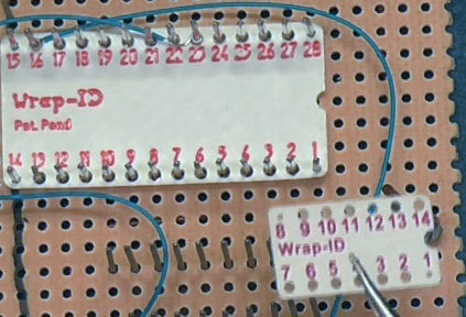
Little slip on tags are available to help keep track of “reversed” pin numbering as seen from the bottom of the board.
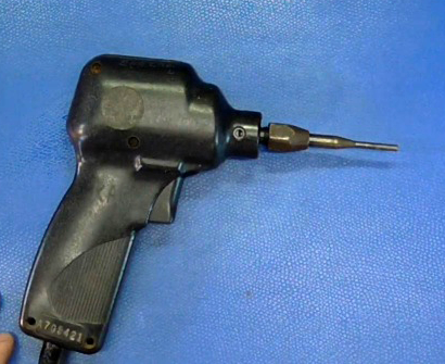
Wrapping a wire on a post is accomplished by first stripping back the insulation on the wire wrap wire to 1″. The bare wire is then inserted into the hole on the wire wrap tool end (that is not in the center), and then the wire is pushed in until it is stopped by the tool. Next the tool and wire is placed over the specific square post being sure that the post goes into the hole in the center of the tool. For a manual router the tool is rotated with slight downward force to keep the wire wrap tight until the wire is completely wrapped, between 5-6 turns.
With the hand operated or power tool the same procedure is performed with inserting wire into the tool, then placing tool and wire onto the post, and finally the tool wraps the number of turns it is set up for.
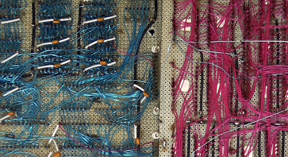
There are different techniques for organizing the wires on a wire wrap board; sometimes the wires are routed together down channels and sometimes the individual wires connect straight across the board in as little length as possible. Both techniques have pros and cons as crosstalk and impedance are affected by wire placement.
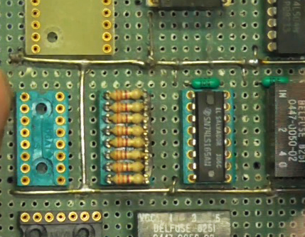
Discrete components can be soldered to headers that then insert into standard wire wrap sockets as shown above with the 3.3K resistors.
And finally a technician named [Jeff] in the old MOS/Commodore R&D lab showed me how his boards never seemed to have much slack in them. He would take one of the skinny wire wrap tools and get on a socket pin/tail, then rotate the pin itself taking up the slack. While this looks better what he didn’t really address was the fact he was making a more pronounced inductor at the end of some wires. The answer to this technique as well as the channel routing technique (the techs would actually lace up the little bundles some times) was that my boards were to be “jungle routed”, I.E. more or less straight connections between pins, and slack was to be dealt with by adding some convolutions in the wire between the two pins by looping over other pins, similar to what you see on a high speed PCB where a trace will take a few extra turns to control the length/propagation time.
I should tell you that [Jeff] threw away my coffee cup one day because of what I had growing in it. From that day until I left Commodore I would make at least one trip a day to the R&D lab to throw his coffee cup away.
[Wire wrap diagram is from the nasa.gov website on Discrete Wiring]


Or you can make a sample PCB for $20 with a built-in perf area zone.
Wire wrap was awful for finding bugs, and practically impossible to fix a few months later.
Do you know what works really well to populate that perf zone? Wire wrap.
Think you kind of missed the point of this…. really you could make a $20 PCB in 1985??? good luck, wire wrap in ’85 was about the only way to go for the sort of board he is showing in the video
Ok, so now we know what was the downfall of Commodore. The coffee cup expenses… :)
Yeah he had to remember to look in all the trash cans every day. My memory is he lost about 3 total where he didn’t find them in time.
I’m surprised he didn’t switch over to disposable coffee cups after a while. Kudos to you for the awesome response to him tossing your cup!
Beginning of the video the board on the bench looks like a Commodore 128? Coincidence? or did he just like having one of his early project around from his day at CBM?
The board I had out was one of three PCB’s that were the prototypes/Alphas for the C128. I had one out as its the next step above wirewrap for better or for worse.
Not mentioned is that wire wrap was measured having 10% of the failure rate of soldered joints(!) Also not mentioned was “dead bug” proto work. Chips were super glued to a substrate up side down, pins sticking up were ready to wire wrap.
At one time, top end computers had wire wrapped “mother boards” which ended up being full sizes mattresses of wire. They could not be insured in those campus riot days unless housed in a windowless brick building. The “beds” were so thick that they were inherently unrepairable, so a single bullet could cost a million bucks.
This old techno geezer still has everything pictured above. It was great technology for one off scientific instrument hacking/interfacing! PC board design code and uber-fast internet pc board turn around have killed wire wrap.
Imagine routing a +4 layer board with black tape on paper. They had cnc machine that you could basically feed a board with sockets and a net list and it would automatically do all the wiring, fast reliable and basically unlimited layers for routing
We stopped hand taping about the time the 4 layers started to become “affordable”. We ere using Scicards running on a dedicated VAX card by the time we did our first 4 layer at CBM.
Totally agree. I did loads of WW for proto-types or one-off boards for early computers. Every wrap has 4 gas tight electrical connections plus WW wire is silver plated. Silver oxide is a conductor so even tarnished connections work. Pins had silver or gold. Great vibration tolerance compared to soldered wires. I have a Gardner-Denver power tool I got at Boeing Surplus and ordered a bit for 0.025 posts and a hand squeezer type for Telco posts. I was just thinking recently about the ease of wiring up steppers and other devices if Arduino shields had Telco WW pins for output.
Don’t forget to mention that every single connection has a inductance formed by the insulated winding(s) and this combined with the good practice of placing a capacitor at the power connections of each chip is a good start for a low noise design.
I still have my WW pistol and de-wrapper tool. Interested anyone?
I did wire-wrap in the 80s. I’m putting together a small lab for fun and $$$. Wire-wrap for sure has its uses in prototyping now, even with $20 PCB boards. I bought the Kayner and inline pins, need the tools. If you still got ’em, I’d like to buy ’em. Let me know. I live in San Diego.
Part of my daily work for a telco is to work on the MDF (Main Distribution Frame) or the DSX1 frame as a jumper jockey. Each frame is terminated with wire wrap connections. We are required to have 8 wraps of exposed wire around the post with one wrap of insulation. I have done this for years and it is still a challenge to get it wrapped consistently EVERY time.
I am pretty sure I am the only tech in the office that attempts to adhere to these standards. Back in the old Ma Bell days there were periodic inspections for quality, those do not exist anymore. I’ve seen as few as 2 turns on a post.
It is worth mentioning that wire wrap might not be suitable in modern day chips as the rise/fall time can sometimes be a bit too fast for it. You’ll see probably see worse issues with bread boards etc.
FYI Just to give some frame of reference: Atmega 328 SPI Master rise/fall time is 3.6ns (typ). So that’s likely what you expect out of their other I/O pads too.
Here are the issues you’ll find in signal integrity for 5ns or faster rise/fall time.
https://www.sigcon.com/Pubs/news/2_8.htm
Some modern chips offer configuration options to reduce switching speed. If you don’t need the highest speed, that can be a useful trick.
I LOVE skew control, especially on programmable logic. :)
Slew?
Couldn’t agree more. I use a 4+” multidrop SPI bus on my own ARM project on a 2 layer board. The best I could do was about 150 ohms microstrips. Normally without slew rate/drive strength controls, serial terminations and SI simulation, that’s much asking for trouble. I played with the combination and the high slew rate/low drive option works out with nice and clean waveforms without requiring series terminating resistors. (I had the foot prints for the resistor packs with cut traces in case that didn’t work out.)
There is always a limit to a technology, or a point of diminishing returns. Controlling impedance with lots of ground plane can get you a little further but at some point even having an MLC cap stretched between the corner pins looks like a cap with two inductors in series and all of the ww pins look like stubs. I start to get concerned when the physical attributes start to approach a quarter wavelength but also you have to figure what the impedance of the various inductors created by the wirings are doing. (and at some point they take on their own self resonance).
However I believe that you could do a wire wrap for a 3.5ns rise time, the boards I was showing had closer to 1ns rise time specs. I am not saying they worked perfectly, but they worked good enough that we didn’t have top go to an alternative.
Also they used to wire wrap ECL back in the day. :)
Sure as heck did. I worked on weapons systems that had tons of wire-wrapped ECL.
Of course ECL was better suited to w/w since it had differential I/o I use a drill to twist w/w wire together to make twisted pairs with about 120 ohms Zo. Also Beldon makes a wrappable coax that has 30 awg center conductors and a 30 awg shield drain. Zo is 93 Ohms. I still w/w up one offs and protos because I can!
I have done dead bug mods with “eye opener” chips on our proto @3Gbps as a proof of concept for the next rev. when we went into SI issue with a certain FPGA vendor. That worked well enough for some cases. Eventually (2 or 3 rev spin) later, we figured the root cause – FPGA substrate (package) routing crosstalk issue by accident – our CM installed a part wrong. Parts of the FPGA didn’t work, but finally all the high speed links works.
BTW we had up to 26 layers PCB and by then further increase in layers didn’t help in routing as vias starting to block routing channels. Because of having to not exceed aspect ratio (via diameter to board thickness), the vias now takes more space. Anyways that board was pushing our PCB vendor’s layout limits and they had to fix it for us. Yes, we had to deal with controlled impedance, dielectric loss at high frequency and even the via stack has turn into stub that we had to drill them out. We have done lots of SI simulations.
I read much later about our OEM competitor quit much sooner in a similar situation and switched to the FPGA vendor. Then the big dot com bubbled blew up shortly after we got the darn thing to work. :(
The million dollar question is – where can you buy cheap wire wrap IC sockets.
I have a project that I am working on that wire wrap would be useful for as it runs at too high a frequency to work on bread board.
Wire wrap was excellent for progressive design. No need for yet another prototype PCB, just make the changes to what already exists.
The other problem today is that have to get everything to DIP or some 0.1″ configuration as only DIP (0.1″) is available in wire wrap, but have to get everything to DIP anyway to use breadboards.
You can do a hybrid of etched PCB (or vector board) with power/ground grid, decoupling and break out. This’ll let you use regular through hole sockets. The vector board have a similar breakout pattern as bread board. You can solder on wire wrap pin posts for the signals that you are unsure of and use point to point solder for the ones that you are sure of. If you need to deal with SMT part – either dead bug or use orange tape on top of the PCB and break out to the 0.1″ grid pads with thin magnetic wires..
This uses the same idea. http://bfreebandingtalktheplanet.runboard.com/t2663
If you have a ground plane/good ground grid, use decoupling and keep the wires close to the plane, you can improve the signal quality. Route the high speed critical clock/strobe signals with coax and terminations.
The techs would inadvertently decrease the impedance of the signals by tightly bundling them which was sort of good and as your link relates, its all about the ground or other low impedance references that relate back to ground. The sort of bad was that crosstalk could increase on certain signals.
The SIP strips and some standard DIPs were sort-of affordable at the Mouser/Digikey. Special connectors however remain pretty expensive. It was typical to take a bandsaw to (someone else’s) PCB and cut out a connector with PCB or even a DRAM/memory area off and patch it in to a prototype for a hybrid approach.
While on the subject… The Ham-radio crowd and in particular the QRP folks often use Manhattan-style construction for HF. I adapted a design by W2AEW and made this:
https://imgur.com/p0VyhrU
The islands are cut with cheapo scissors out of the same single-sided and very cheap PCB material as the ground plane and glued down to it with ordinary household polyvinyl acetate. – I would very much like to know it’s strengths and weaknesses, and when I should opt for some other construction technique.
The copper tape is also cheap. I wonder if I could make good quality microstrip and IC footprint stickers with it, somehow… Any feedback on this idea?
This is a great technique, and like any technology with the word microstrip in it, its cognizant of the source and load impedances and the dirty details of coupling and transporting the signal. Alan does a great job of keeping this tech alive.
The idea that you could print an outline that when matched with the right tape would form a mixing stage with the right impedances is very cool! Imagine a version of “Colorforms” (ever present in the 1960’s when taking an extended car trip) where each symbol coupled with the right parts makes a stage such as a 1ghz inverter, etc.
So to answer your question its a _good_ construction technique thats only issue is the way it looks (but hey, thats the price of hi frequency). Things I built early on using “3d jungle” techniques also resembled the late great Robert Pease which often turned out to be a reliably working model that resembled a hairball. But it was a working hairball!!!
Where do you get this cu tape?
I ordered it from here:
http://www.aliexpress.com/item/40MM-X-30M-Conductive-Copper-Foil-Tape-Free-Shipping/838170796.html
And thanks for replying! – Very encouraging! :D
The most robust way to get high-accuracy cu stickers from tape would probably utilize a difficult-to-manufacture die to punch them out… Applying them to the PCB without distortion might be done in the same way as one applies tattoo stickers; with a supporting film on the front.
Laser cutting could also work well since the material is so thin, if one has access to one of those.
Use a vinyl cutting plotter? Or find pre-cut copper tape with fixed width.
Get the right thickness of single sided PCB and stick the copper tape on the side with FR4 and you are all set.
A vinyl cutter might work very well! eBay seems to have them a lot cheaper than Aliexpress, oddly enough. This must be thoroughly researched. :D
Careful – the copper tape used for EMI has conductive adhesive. You need uninshuled FR4 touse that, I would think
How about using think .03″ single-sided copperclad and a (robust) hole punch for the pads?
uninsulated….
or flex instead of fr4
Thanks for this! As a relative new comer to electronics who scrounges and recycles as much as possible I come across wire wrapped boards from time to time. This history lesson has cleared it up for me.
Great Video Bill. Always good to see your articles.
Thanks. We need to create a way to take suggestions for future videos in case people have a particular topic they would like to see abused.
Here’s some that I think would help those born to the digital age. I often see a lot of code and several MIPS replacing a capacitor and resistor so I think some analog explanations would help.
Some ideas –
CR time constant
CR filters – low pass – high pass – band pass
OP amps and configurations – newer SoC’s have these analog components, input impedance and the cause of offset don’t seem to be well understood
Wheatstone bridge – accurate measurement
Wien bridge – accurate filtering / measurement
PLL – many newer FPGA now has PLL
Although digital solutions such as DSP are easy to do now they’re not always cost effective especially when the core function of a design only requires a low power uC and you have just one complex analog input.
A series on sensors would be useful to, basic stuff like type ‘K’ thermocouples, CCD’s.
I thought about these when HAD was calling to writers but I don’t have the experience with software to make the pretty graphs that should accompany math based explanations like this.
The late (great) Bob Pease of Nat Semi would laugh at people going to great lengths to use a computer to perform simple analog functions. Even a common LM741 performing a filter function can outperform a very pricey DSP chip.
There are high-frequency, high-efficiency magnetic amplifiers in some new computer power supplies. The tech is largely unknown today in spite of supposedly impressive performance figures and info on it is difficult to come by.
I would like to see some “Retrotacular” stuff where you dive into the design of some of the Commodore machines and going through the design decisions, etc.
I cut my teeth so to speak when I was 5yo on the C64, password “protecting” my dads chess game, from there, launching my IT career and electronics hobby, so having this insight into the how and why the CBM machines were the way they were would be awesome.
20 years ago this was very common in the interface devices we used on our test benches. Thanks
Used a wire-wrap gun mostly in my time working at a telco in the ’90. Handwrapped connections where said not to be the same quality of basically micro weldings and only allowed for quick repairs when the machine tore the wire.
I would agree with this. There are things like continuous torque, etc, that a human can not do.
Did way too much wire-wrap in the late ’70’s as a technician in the US Navy.
Massive electronics cabinets and consoles had doors in the back that would hinge open with logic cards plugged into the front, and a rats-nest of wire-wrap interconnection in the back. In tech school the instructors would short, open or mis-route ONE wire (or pair), and we’d have to find and fix it. Doing system upgrades at sea were even more intimidating (remove these hundreds of wires, relocate these cards, add those cards, add hundreds of wires).
I still have nightmares… So glad I switched to software.
But damn, was I ever good at it. Best music to wire-wrap to: Steely Dan
Wow. Were you assigned to surface warfare ships, or subs? Oh and when it comes to music, I’d rather work to the sounds of music by Grieg.
Great video as usual. My only complaint goes to some camera shots with moving object + moving camera thus moving background.as well. Brought memories of Battlestar Galactica. …Ouch!:)
Yeah,that was a bigger issue than normal, I need to find a better answer. You can see where I faded to a still image several times just to reduce the vomit factor.
You can easily make your own wrapping tool if you just want to play around with the technique: http://ao2.it/102
It won’t be as good as a dedicated one but it can still be useful sometimes.
I made one for temporary use and it was publushed on hackaday back in 2006:
http://hackaday.com/2006/07/20/improvised-wire-wrapping-tool/
I’m sorry to say I’ve misplaced the original pictures. I used a small screwdriver ( with the same rotating end as some real wire wrap tools ) and stuck a 1″ section of plastic ink-pen tubing on it with a small chunk of folded metal cut from a 3-1/2″ floppy shutter to separate the post and the wrap wire. It worked quite well in a pinch and actually looked pretty good. You could also pop off the plastic tube and use it as a screwdriver again.
Wire wrap wasn’t JUST used for prototyping. I was on a VLS (Vertical Launch System) submarine in the early nineties. The VLS is a method of launching Tomahawk missiles, and there were five large cabinets that had wirewrap backplanes. These backplanes were HUGE (~4 foot tall & 2 – 2 1/2 foot wide). They were so completely covered with wire that you couldn’t see any of the board underneath. The wirewrap posts had a board to cover it when connections weren’t actively being changed. Changes were only made by contractors while the sub was in drydock, and only when system modifications were necessary.
I don’t know if it was only the submarine that I was on (we were a special projects boat; which is a ship that gets “experimental” equipment and such), or if all the submarines that had our particular system (CCS Mk 1 Mod 3, if you are interested enough to Google it). IIRC, there were only six submarines that used the CCS Mk 1 Mod 3 weapons system.
A technique I used a few times was to use a double sided copper clad board as the substrate. I would clamp a perf board on top of it, using the perf board as a drill guide and drill out all the holes I needed for sockets, then I’d toss the perf board. Next, I’d remove the copper away from all the drilled holes using an exacto except for where I wanted to connect power (one side) or ground (the other side). Then I’d mount he wire wrap sockets in the holes and raise them just a bit so I could solder the top plane to the power pin, and flip the board over and solder the ground pins to the bottom plane.
After that it was just the usual wire wrapping job. It made for excellent low-droop/ground bounce power feeds.
One of the boards I did was a 68020 + DRAM + a bit of PAL logic which plugged into a legacy 68000 system. Considering the grid of power pins on the 68020, I don’t recall now how I soldered them to the top power plane, but obviously I did somehow.
Nice! While reading the article, I was just thinking about exactly this — “wonder if anyone’s used double sided copperclad for power / ground planes”
I wire wrap In-Circuit test fixtures every week just about at work.
Anywhere between 50-500 wires per fixture, from receiver to pogo pins, all done by hand. About 50/hr. I prefer the channel/column bundling technique myself. A lot easier to find test points and broken wires than point to point rats nest.
If someone could give me a cnc wire wrapper for free that would be great. I would settle if someone made an augmented reality or ipad app showing where to wire. It is time consuming to find your test point and is easy to mix or skip one.
Use a PCB layout program, to make a layout of the test fixture, map the schematic to it, and use the net highlight function.
Wire wrap was a major part of our college hardware lab class.
I also remember a special type of wire-wrap wire that didn’t need to be stripped; the corners of the wrapping posts were sharp enough to cut through the insulation and make a good connection. This was really handy because multiple connections could be made with the same piece of wire. I have no idea if it’s still available.
““reversed” pin numbering as seen from the bottom of the board.” REVERSED?? No, that clockwise numbering standard is the original Octal Tube Socket with the numbers right in the phenolic, like DeForest intended it! :-)
I still have my electric wrap gun from Gardner-Denver which made the wraps on the backplane and circuit cards for my 1974 6502 based homebrew computer. In 1967 I watched IBM 360’s being built with automated tape-driven WireWrap machines in Poughkeepsie. In 1977 at IBM I had a fulltime woman technician who did wonderful work on test systems I designed. 20Mhz+ bit-slice microcoded machines that created the address and data sequences for testing ran clean. All these boards had good power and ground planes with preinstalled pins every inch and bypass caps every 2 inches or so.
But the fun continues with Arduino, and I collaborated on the design of this derivative board: http://arduino-info.wikispaces.com/YourDuino-RoboRED (You’ll notice a LOT of square pins that COULD be wirewrapped. I have shipped over 1000 of these boards and I bet none will ever see wirewrap.).
No, I’ll wirewrap on one tomorrow, just for Nostalgia.
Regards, Terry King …In The Woods In Vermont
Recently picked up a used electric wirewrap gun for £25, 250m of wirewrap wire for £3 and a pile of over 100 6-40pin gold-plated sockets for £12 from a certain site. I am probably the happiest 45years+ sad old git in the UK. Why you ask? Because I want to do something that I dreamed of doing during my childhood but could never afford!!. Nostalgia is a powerful force and I’m dreaming retro!!
Cheers
Holy crap that’s a lot of right-angle traces on that C128 board….. Did we not understand their effect in the 80s, or….?
or … in that era — TTL inputs needed quite a bit drive current so inputs acted like a dampener or termination. At the same time the buss speeds were so slow that you wouldn’t see much of a signal reflection from right angle trace.
By ‘TTL’ I mean the original 74xx, though you may see some 74LSxx.
Don’t forget RTL, DTL HI-NIL and CMOS. I wire wrapped up an NS 32032 CPU with 1 MEG of main DRAM. The memory chips alone cost over $1000. Still works but seldom play with it.
Great intro to the lost art. I’m wondering if anyone’s tried twisted-pairing the wires to prevent x-talk etc – would make rewiring painful …
Been there done that. Labor intensive and slow to do but actually works well if ends terminated in Zo.
I still use wire wrap occasionally to jump from board-to-board when building up a prototype. its great for jumping between devboard headers. I do agree the rats nests we used to build with discrete processors, srams, eproms, 7400 etc was a mess i never want to go back to ;-)
Thanks by this great post Bil! You have motivated my to make a cheap wire wrap tool I left the link for anyone interested http://chemary.com/2014/12/31/make-you-own-wire-wrap-tool/
I stumbled across this link and enjoyed reading it all !! It sure brought back some good memories. Back in 1979 – 1985, Charlie H. and I would be given a new “Universal” Augat or EMC wire wrap panel. We would generate Fortran code that would generate X/Y coordinates from net list that could be input into our software. The software could generate card decks for running Gardner-Denver Semi-Automatic (We had 2) machines, Vertical Automatic machines (we had 2) or the larger Horizontal machine (one). Much of the computer-rack Oil Exploration gear we manufactured used dozens of Wire-Wrap panels. We also wrapped smaller panels for prototype boards for other TI divisions.
Seven years, I programmed those machines as well as the 2 Omni Testers we used to test the wiring.
Thanks for the memory jogger !!
I noticed, on the boards in the video, you made some power and ground ‘busses’ out of some thick wires that ran around the board near the ICs. How did you connect your ICs and components to those busses? The bus wires don’t look like they have wire wrap pins coming off them.
I’d like to know this too.