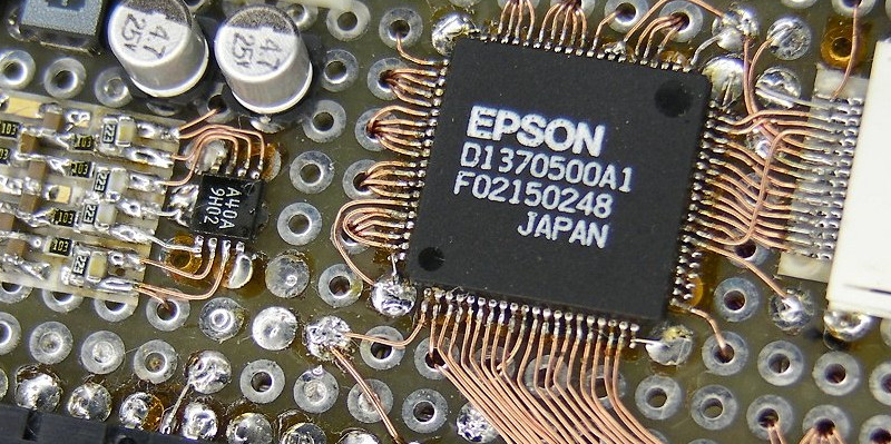
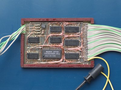
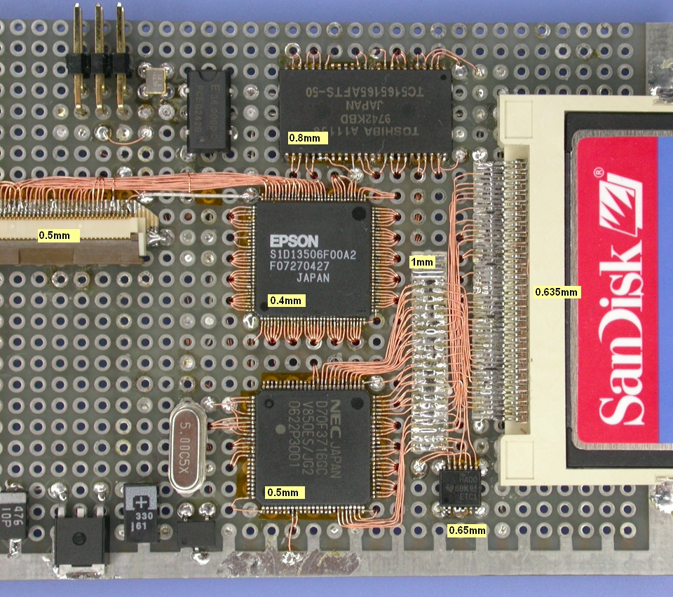
Back in the 90s when surface mount components gained widespread adoption, the quick and cheap PCB prototyping services of today were unavailable. This led many to develop their own approaches. In Japan a particularly novel and beautiful approach was, and still is, somewhat popular. [NE555]’s work is a excellent example of this technique using a fine enameled wire (you can find this on eBay as “magnet wire”), wirewrap board, and careful hand soldering. [NE555] has made a great video on the process (which you can watch below).
In [NE555]’s video a relatively large tip is used. The ICs legs are pre-tinned, and the IC is glued to the board, with Polyimide (Kapton) tape insulating the legs. [NE555] uses a self-developed wirewrap pen as an aid when connecting pins. There are some details of this process in English available. Aside from this, fairly standard tools are used. The fact that [NE555] uses quality Hozan brand wire cutters likely helps with the precision wire trimming required.
What’s quite shocking for me, is the [NE555] uses no optical aids. Most of my own SMD rework take place under an inspection microscope, but clearly [NE555]’s years of experience allow the process to be completed by eye. A microscope however is used for final inspection. While techniques like these maybe slowly replaced I can’t help but admire the craftsmanship and tenacity required to construct these beautiful prototypes. For more examples of these wonderful boards, check out the pictures and video below (and follow NE555 on twitter!)


That’s straightup beautiful.
http://hackaday.com/2016/10/10/ne555s-smd-prototyping-is-a-work-of-art/#comment-3227113
AC stands for ‘ass clown’, does it not?
Video blocked in the USA, can’t see any of the prototyping goodness.
wtf?
It’s got some J-poppy type stuff playing, maybe licensing issues.
I think I found one that works. Please let me know if it isn’t the same; proxy servers don’t seem to work for the YouTube version and I almost downloaded malware on another site that claimed to have the video.
http://www.dailymotion.com/video/x2zbblt
I have a friend in CH who verified that this video is at least mostly the same content.
The link works for me using TorBrowser.
Tor warned me off, Youtube was trying to extract HTML5 data to identify my browser. I think I could just download it through Keepvid.com, but I’d need the Seamonkey plug in for Firefox and Keepvid’s Helper plug in. At this point, it isn’t worth it. This is just one more reason to switch to VidMe, Daily Motion, etc.. If you want crap like this to go away, you have to stop buying it.
Yeah I can’t view it in New Zealand
I used offliberty to rip the video. Amazing!
Use the Tor, Luke
that work is a miracle.
Un-freaking-real. That’s not only art, it’s absolutely amazing.
Hard to choose a phrase to praise. All understatements.
Just… wow. That is a beautiful. Really shows off the talent of the mind and the hands.
That wire- is it the same stuff 1/8″ headphone / mics / aux cable is made from?
PTFE coated wire. I think headphone wire usually is stranded differently though.
No, No PTFE.
PTFE will not melt with even your hottest soldering iron.
The wire used is usually called “enameled” but it usally 2 or more layers of coating of different composition. Polyester / Polyurethane / other.
https://en.wikipedia.org/wiki/Magnet_wire
Waste of time
Please explain why you think this is a waste of time?
Please don’t feed the trolls. :-)
Though it’s a very Zen full work of art I also believe it’s mostly a waste of time.
The combination of today’s PCB fab prices and the state of art of PCB software means that the amount of human time involved in designing a pcb for this kind of work is less dan soldering even a single bord wire by wire.
And if you want more then one you want to have a PCB design anyway.
Even when hand soldering on a pcb you can position and solder a 64 pin TQFP in 20s by dragging a blob of solder across the pins.
Compare that with 8 minutes into the video where [NE555] has to resolder 3 wires because he accidentally touched them while soldering a single wire. The unknown amount of flux left makes these connections error prone and unreliable.
Where on earth are you coming from.
Why learn machining when you can find a mass produced equivalent of a component that you’re looking for?
I suppose you would disapprove with the practice of home PCB fabrication too?
Professional PCB fabrication certainly has its applications. However in this scenario it’s more of an art. And a meaningful one too.
Say you wish to reverse engineer a product, And would like to quickly break out a connector/IC
Also, CAD programs can often be a learning curve for some.
Stop to question the activities of your own life before calling that of others a waste of time.
Many hobbyists actually have experience with PCB design, CAD software, and fabrication. There are entire communities dedicated to home CNC machines which allow for fine enough tolerances to allow for QFN32 chips to mounted on a home built board. The electronics community has been growing and evolving for decades. Why get stuck doing an archaic art when design and fabrication time using machine controlled methods is more than twice as quick? Also you can literally buy break out boards for any chip size for pocket change, just buy a bunch and keep them on hand. Practical solutions to problems that generally aren’t problems anymore.
Cut the arrogance and learn 5 solutions to every problem, because you’ll reach the day when 4 of them don’t work.
Well, I think people call it a waste of time (I certainly would never do it) because I want the ASSEMBLY so I can FINISH more than I want to enjoy the ART OF MAKING the assembly. It’s all about where you derive satisfaction, the technique of making stuff or having the final idea in your hand so you can improve it or move on. My guess is for most of us where getting protos out fast and on time is a job too, we immediately also turn our noses up at this sort of thing. I believe in other artisanal things like cookies, but not PCB’s – I think it’s certainly a minority opinion.
I also dont believe much in home 3d printing either (I just buy all my prints from a chinese SLA supplier that is lightning fast and cheap in one color). The prints compared to even cheap SLA are just terrible, having sampled the gamut of services as an engineering manager. I would rather dream more about WHAT I could make rather than HOW I will make it, especially in the age of dirt cheap centralized, fast prototype production.
That being said, home machining still makes some sense to me for milling out PCB’s and also milling parts, milling hasn’t gotten extraordinarily cheap these days. I just so rarely need aluminum anymore.
Regardless of whether you get satisfaction from process or results, I still challenge the claim that this is a waste of time.
1) Both processes – the semiautomated method of entering a schematic on a CAD system, laying out a PCB, mounting the parts on the PCB and soldering them, and the manual method of drawing a schematic on paper, arranging and mounting the parts on a bare board, and wiring them – take considerable time. So IS the semiautomated approach actually quicker? I doubt it. Even using an autorouter, well, many people don’t even bother with an autorouter because they end up spending almost as much time cleaning up the results as they would have routing by hand.
2) There are learning curves for both, which I submit are much longer for the semiautomatic method. I’m not just talking about learning the software; I’m talking about getting solder stencils made, finding and dealing with fab and assembly contractors, learning about design for manufacturing, parts purchasing, and all of the other details involved in circuit building.
3) The chances for error may be somewhat higher for the manual method, but I think this is offset by the cost and time for fixing the errors, which is generally much higher for the semiautomated method since it can involve scrapping the board and all of its parts, while most errors in manual building are easily fixed, and many are detected while building, because “hey, there shouldn’t already be a wire on that pin”. I’ve never seen anybody doing a manual build place a component on the wrong side of the board, or use the wrong footprint for a part.
I’m not even bringing turnaround times into this because the two methods have different application sweet spots: manual build is suitable for making one or two items, while semiautomated build is better for larger quantities. Unless you are making something for a client who expects to see a manufacturable prototype, I submit that making a single board using the semiautomated process is a huge waste of time. And while NE555 has obviously developed some wicked skills that probably took many projects and years to refine, I doubt that his method takes much more time than any other manual build method. With any method you can do a slop job or make something that people will call “a work of art”. And that goes for semiautomated builds as well.
By the way, I’m calling it a “semiautomated” method because there are so many steps in electronics building that even today require human expertise. Is there a schematic generating program that can accept a netlist and generate a readable schematic? I don’t think so. Is there a PCB layout package that can take a netlist and a BOM and produce a practical board layout? I don’t think so. Even at the parts procurement level, having an assembly house do that just shifts the human interaction to a different agency, unless you’re rich enough to just send the BOM to a single vendor and trust that they’ll give you reasonable prices. I’m not saying these things COULDN’t be automated, just that in 2016, they aren’t.
This method works for NE555 and he clearly enjoys doing it (and I enjoy looking at the results).
I always find it strange when people want to say “no… this is a waste of time!” when they’ve not been asked to comment on it’s efficiency. You can use it, or not (personally, I’m planning to adapt this technique and use parts of it when I’m doing SMD rework). But we don’t know NE555’s situation, and we’re not in charge of NE555’s work… so… why not just take what you can from it and leave it at that?
You or I might spin a board (and wait a couple of weeks), but that doesn’t mean that works for everyone, or everyone should do exactly what we do.
Yeah, if this is a waste of time then art is a waste of time. Maybe you just need to consider that other people’s perspectives and impressions are valid.
on what planet are you on and what magical plant are you smoking on it?!
its called prototyping for a reason? Prototype kind of implies that reliability is not its strongest point!
If you have keen eyes, and patience you can easily spot the stray solder blobs between the pins?
Flux yes, ok there may be some mirgartion issues with the excessive amount, but a bit of IPA of Flux-off and it’ll be good!
The most expensive route (getting PCB’s fabbed out of house) isn’t always for everyone!
I’m sorry I forgot to mention this is a very Zen full work of art.
i will abstain from feeding anyone, with one execption; this unit is most likely MUCH more mechanically sound, provided the usual “goop”/”crud” is used to finish glueing each part in place BY HAND after the soldering. on a normal SMD board the springy glue would not aid a thin trace in schock absorbtion. but with this board, you could pot the entire thing and it would survive being dropped from a higher height then consumer stuff.
if my skills were up to that level, i would ALSO spend DAYS assembling such a thing just to frame and mount on the wall… complete with flickering status LEDs… andor a backlit LCD like [NE555]
As an art project, it’s nice and challenging.
As a prototype, unless you absolutely don’t have access to PCB technology, then it’s a waste of time because:
– It will take days, sometimes weeks, to wire just a few chips.
– It’s a very tedious and boring work.
– You need to have a schematic on paper, and mark on paper each pin you wired. Otherwise you may forget some pins unconnected, or you may miss some wires entirely.
– After too many hours of wiring, you will start making mistakes, and put a few wires on the wrong pins or on a wrong chip.
– Debugging will be way much harder, because of possible missing or misconnected wires. The advantage here is that you can wire small blocks and debug them step by step, while you wire.
I learned all these the hard way, back when there was no other way:
https://cdn.hackaday.io/images/2572221402262586660.jpg
Designing and ordering or even manufacturing your own PCB is much faster.
I’m sorry you’ve had such bad experiences with prototyping. In my experience, it takes about the same amount of time to lay out and route a PCB as it does to build a prototype. Seriously – it takes me the same amount of time to run each piece of 30 AWG Kynar wire as it does to run the same trace in any of the PCB packages I’ve used.
Of course, if you want to make more than about two of something, then you’ll want to do a PCB anyway, which means you still have to spend the time on PCB design. But prototyping still gives you some advantages:
* Extremely quick turn-around – as I said, you can have a complete circuit in the time it takes to do a PCB design, to say nothing of the time it takes to get it fabbed.
* Most prototyping techniques, like deadbug, manhattan, and whatever NE555 calls this, make it relatively simple to rip out part of a circuit and redo it without throwing away the rest of the circuit.
* Developing the skills to do this kind of work is useful when modifying circuits on PCBs.
* Cheap, cheap, cheap, cheap, cheap. PCBs are priced by the square inch. Bare copper-clad or perfboard costs a small fraction of any fabbed board.
* The cheapness in both $$ and in time means you can build things that otherwise might not be worth trying.
* Never accidentally use the wrong package footprint or place something on the wrong PCB layer. Don’t ask me how I know this.
* Never accidentally make your own footprint that shorts a pin to the power and ground planes. Don’t ask me how I know this one, either. Fortunately it was fixable by drilling out the plated through hole, as it was about a 12″x10″ board.
* Debugging is actually easier (with deadbug style prototyping) because everything is on the same side of the board.
* Schematics don’t need to be formally entered into a design package – hand-drawn on paper works just as well. This is another time saver.
I just can’t imagine doing a one-off project on a PCB.
Regarding above comments:
I know that it may be out of scope for the typical home user, but Altium really can do a lot of the things you are describing. of course, YMMV, but for me altium was like 10x faster than Eagle – I tried eagle a few times, and it always left me wondering, why the hell do people use this? You get a nice BOM, schematic, and files that pass at the board house first time. I can understand your position if you are using Eagle or FreePCB – but even complex boards are pretty fast in my experience with good engineering tools.
Also – just adding a few vias and cut points is pretty easy (you usually don’t have to add much after the router). I would gladly rather have my weekend time back for $25 and 3 hours of setting up for the PCB house as a late night during the week. I tend to add 1-2 vias in the middle of autorouted traces as a cut point for most nets so I can just dremel it off if I have to, just pop pop pop at the end. That way I can use the via as a cut point and jumper via to via with a bit of wire easily if I screwed up the ratnest. This gives the flexibility I think most people are looking for, especially with so many connections. This gives you a really high chance of getting a working board back in 3-4 days, with the added advantage of being able to rerev and send again once you are ready to make 10-20 asms next time. I highly recommend this strategy, modern tools are worth trying out with a few tricks like this! You can always remove this sort of garbage in the next rev when you get it right, haha.
When it gets down to it though, corporate life really taught me the most important lesson: Focus on designing to solve your problem, less on making logistics. these days there is always someone much better and cheaper than you at making stuff, especially these days…
Your comment is a waste of time
Man, I really wanted to watch that video. Not available in the US.
How about now? I couldn’t watch it either but maybe the alternative one above works.
Works fine in the UK.
I want his tweezers. I have failed to acquire a decent pair these many years. One time I paid $20 for what were supposed to be good quality electronics tweezers and they were identical to the marginally useful ones you get in a $5 soldering accessories set. I hate ordering stuff like that online, unless you can eyeball it, feel it in your hand, you don’t know whether it’s crap or not until you get it.
Tweezers brand name is “Hozan”. He even show the type number in the video.
“Erem” also makes good quality tweezers.
I was going to mention Erem’s, too. I found a few from an electronics surplus store about two decades ago when I was still a student in (or maybe right after) college. I paid more for those than the cheap-o stuff, but the Erem’s are so much nicer to work with. If I had known then what I know today, I would have bought a handful each of the flush cutters and the mini-pliers just so I don’t ever have to use the cheap stuff. They are wonderful.
Another thing that you could look into are the ones used to build coils for vaping. They have ceramic tips so they can touch glowing coils without shorting them out. A little expensive, but not too bad.
Try Wiha.
Wiha arent exactly known for cutters, maybe you meant Knipex?
Ohhh not go down this road my friend. I’ve been there and tweezer addiction is a horrifying thing. There a shop in Akihabara called Hirose technical. If you ever find your way there… beware.
My favorite tweezers are made by Rubis. The Rubis SS-TNFs are slim titanium tweezers they’re light and have a very fine point ideal for SMD rework. I once dropped a pair on a wooden floor. The tweezers were undamaged, but embedded themselves straight up in the floor. They cost about 50USD.
Idealtek also make great tweezers. They’re probably the most well known of the high end tweezer manufacturers. I have fine pair of cermanic tipped Idealtek tweezers. The nice thing about these is that the cermanic doesn’t conduct heat, if you’re soldering this means you don’t loose heat to the tweezer.
Now the tweezers from Shenzhen. There are actually some pretty solid tweezers coming out of Shenzhen these days… the problem is that they’re all marked Ventus. And generally Ventus SS-SA (SS-SA is actually a designation used by a decent Idealtek tweezer). But all Ventus SS-SAs are not created equal, it’s really hard to find the good ones online. The only way I’ve been able to do it, is to go the the markets themselves… the good ones cost about 7USD in the markets.
Anyway… here’s a video I made about tweezers: https://www.youtube.com/watch?v=l8l-aNsmcgU
There’s also a really interesting tweezer mod I found a while back, I should probably post that on hackaday at some point.
LOL!
“the good ones cost about 7USD in the markets.” …plus the cost of a trip to Akihabara. Or Shenzhen.
This resembles the incredible projects that came out of ELM-CHAN. I’m convinced these guys are cyborgs.
http://elm-chan.org/he_e.html
That’s what I was thinking about ….
NE555 = elm-chan ?
Twitter links to elm-chan on the left.
Yes 1997 page from elm-chan updated a couple of years ago with the videos if I’m not mistaken.
http://elm-chan.org/docs/wire/wiring_e.html
This guy is amazing, love his works and prototyping style.
Yes, maybe elm-chan can comment. But I think NE555 and elm-chan are the same person.
well, I have never seen them both in the same room at the same time.
so, there’s that.
Amazing stuff, thanks for posting!
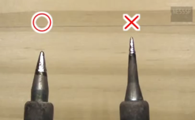
wow so awesome makes me want to try myself. i don’t get why he uses the big tip thought. OK as you guys said heat capacity maybe but how about higher precision on the smaller tip?
Higher precision is not going to help after all your flux has evaporated.
Flux dissapears relatively fast with this method because you have to use a higher than normal temperature to burn the coating of the wire.
Using 2 soldering irons could help. a thick tip for wetting the wire and a thinner tip for the actual soldering.
Exactly. At my workbench, I have two standard Hakko 936 soldering stations with a standard and an SMD iron, a cheapie Chinese iron (for abusing), a Hakko 808 desoldering gun, and a hot air reflow station… And I could never go back…
I’ve tried carving my own tips for delicate work, and yah, you go too small and delicate and the heat dumps out of it too quickly… gotta keep it between about 45 and 60 degree angle pointyness… then the sharp end rounds off rapidly and you end up learning to cope with a tip bigger than what you’re soldering by exploiting surface tension of solder.
high thermal flux irons can help mitigate the thin tip issue but are usually very expensive, i drop by the various importers or brands at conferences to play with gear i could only wish to own privately, among my favourites are the new JBC stations, they heat up in seconds and i especially love their solder feed gun, it allows manual feeding and retraction in a very ergonomic package, i haven’t used solder feed guns from anyone else so that might be true of any feed gun.
I like how he uses all three hands to tin the leads
It’s Japanese, those hands are probably tentacle-articulated human-like gloves.
Youtube video has been DMCAed.
This is getting fucking ridiculous, it’s time there’s penalties enforced for false DMCA claims.
That’s youtube’s “Democracy” at work :^)
Kind of like a religious video.
Everybody can have a say on behalf of the topic, But nobody is left satisfied
as the original content did not change nor the individuals absurd viewpoints.
It was probably the music
Doesn’t help the fact that youtube’s content analysis team (which I think It’s completely automated)
is corrupt as hell.
Can an algorithm be corrupt? As in morally deficit?
Yes. Ask failbook/suckerberg.
@notarealemail
LOL
i.e the mass surveillance engine.
Beautiful but not useful. I mean, imagine if (or “when”) one of those things fail due to broken soldering or stuff… the debugging must be horrible!
True, but people like [NE555] just smile and grab their electronic repair kit!
I know I smile everytime my gas grill malfunctions; cheapo is going on ten years, pretty soon everything will have been replaced so is it even the same grill anymore? ;)
False. What makes you think that finding a cracked solder joint on a reflow-soldered board is any easier? Trust me, it isn’t. When your connections are discrete wires, it’s pretty easy to find the broken one because it moves. On a monlithic PCB, broken joints are much harder to find. And of course it gets nearly impossible where BGA devices are involved. And yes, BGA joints do fail. I’ve seen it.
Tan-fastic. Has anybody found any examples of this kind of work done with BGAs???
You mean like this one:
http://www.thekirchners.net/rebol.jpg
?
OMG – forget I asked.
OK, sure, no problem. But just in case you’ll change your mind:
http://i66.tinypic.com/2brteh.jpg
:o)
*jaw drops*
I can’t imagine trying to fix that ‘if’ it fails. Probably pull it apart and start from scratch!?
Tan-fastic? Michael Rosen?
Hmmmm, (click) noice.
This is complete awesomesauce !!!11!eleven
Compared to his work , my crapwork stays crapwork
https://imgur.com/EhUnBaf
Lol, I’m just pissed that you got an Imgur link to work! :P
hackEDaday lol :D
I’ve been reading up on this the last week by coincidence, and just got my spool of magnet wire to give it a try (I got green-enamelled stuff so hopefully it’s more obvious which parts are still insulated). I have had a Z80, SRAM etc sitting around for a while that would be fun to try it with.
The other site I found about this is here: http://info.ee.surrey.ac.uk/Workshop/advice/grotwire/index.html
They talk about wiring channels, which look really neat – like tiny wiring conduits with slots to run between the ICs. Anyone know where those come from? The reference on the page is to the internal inventory at Surrey Uni (and a dead link too).
Oh sweet!
So have I. There are a ton of resources on behalf of the z80 as it’s very well documented.
Personally I’ve been collecting bits and pieces all over the past several months or so.
Fell free to contact me and I’ll help where I can.
Cool – I’m working on two z80-related projects very slowly. One is a soft-core in an FPGA (FPGA vt100 on hackaday.io) and the other would be a real hardware z80 just to play with. I’ve always wanted to make a small z80 single-board, and now memory is cheap and flash makes the eprom part easier too. Real Life has got in the way, but I can see when I might have some spare time again soon…
I believe Grant Searlie has a z80 based FPGA project,
And leaves the rest customizable.
What’s funny is that the FPGA he uses runs at 20 MHz.
You can buy a 20 MHz z80.
Yes, it was his project that got me started. It’s not his CPU though – that’s yet another project called T80. You *can* get a 20MHz Z80 (the FPGA runs at 50MHz in fact), but you can’t implement VGA, serial chips, etc etc with no extra external logic with a real chip :-) (Just add level shifters for serial, and a DAC for VGA). Writing my own VGA text mode hardware and seeing the z80 writing to its screen RAM for the first time was good fun.
@Howard Jones
You’ve implemented a discrete graphics controller?
If so that’s very impressive. It was common amongst
Japanese consoles or systems from their origin much
like the turbografx or X68000. If I can recall few hobbyists
Today actually wish to implement graphics controllers into
Their home brew 8 bit builds like Mathew Sarnoff and his
6809 machine. It would be interesting to say use a 6847 for graphics.
Personally I’d really like to see say the DMA module implemented.
Graphics Controller is a bit fancy – it’s text-mode VGA :-) It’s not that hard to do, once you figure out how a CRTC normally works. I do actually have a vintage 6845 that I got to go with the hard z80, and a nice early 80s CRTC book.
The fun stuff is games console-style graphics. I was reading old siggraph papers today about hardware scaling and rotation. That stuff would be cool! For basic graphics hardware there are things like the annotated Q*Bert arcade schematics, which show hardware sprites and background tile rendering. Also check out the Vulcan-74 done in only 74-logic and SRAM. This stuff is where the FPGA makes things a lot easier though – prototype changes are all in the text editor.
I’ve seen this stuff used to line holes (of various shapes) in sheet-metal… like where you pass wire-harnesses through a metal case, the plastic slotted “channels” in those images wrap *around* the metal’s edges. This is an interesting use for that stuff!
http://info.ee.surrey.ac.uk/Workshop/advice/grotwire/xmpleBd_ss.jpg
Oooh, like this stuff?
http://www.cableorganizer.com/richco/grommet-strip.htm
“vero wire” will give some results for wire spools (lower temperature?) wiring pens & plastic combs
https://en.wikipedia.org/wiki/Wiring_pencil
Steve Furber is also showing off some of his Vero Wire techniques with one of the first arm prototypes at 0:24:00 into this video:
https://www.youtube.com/watch?v=_VYxIaw1kBU
I would be hesitant to put magnet wire into channels like this. Magnet wire has VERY thin insulation, so running wires in tight bundles over any significant distance is going to capacitively couple them to each other, more than I consider healthy.
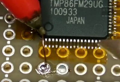
Excellent stuff! Nice to see the skills involved. Kapton tape is polyimide, not nylon (polyamide) by the way.
Nice work, shame on the naysayers though.
I got this enamel wire a name at work as “USB Wire” due to the amount of expensive boards recovered from a customer hotswapping 24V powered printers amongst other things.
I’d reroute an unused USB data track to the burnt out port and cut the dead tracks. Yet that is nothing like this!!!
BTW I save the co. around £50 to £400 depending on what board!
That’s awesome work!
As for all the ‘just get a PCB fabbed’ nay-sayers… first, it might just be that he enjoys doing this. Seriously, do you ask painters why they don’t just snap a picture with their cellphones?
Second, I wonder how much rework the nay-sayers do on their boards. Obviously the initial labor investment ne555 puts into making a board is massive. After that… What if he wants to move a wire, change a few connections around? It’s a piece of cake for him. Compare that to fixing a PCB design, paying and waiting for the new board to arrive. Then, do you throw the original away, go with all new components? Or do you try to desolder them. No doubt the passives and common aren’t worth desoldering, any specialty parts on your boards though?
I’m thinking the cost/benefit ratio of doing real prototyping vs purchasing a fabbed PCB is probably quite a bit different between when your project is mostly taken from the reference design on some chip’s datasheet and the innovation is primarily in software vs the opposite. Maybe there is a different best technique for each situation.
I love all the cutting edge tech we get to play with these days but I’m also kind of jealous of the 1970s hacker/makers. I wish we could get these new parts in through hole designs and pop them into mass-produced, inexpensive wirewrapping sockets.
Don’t over-romanticize the “good old days”. Wirewrapping sockets were NEVER cheap – they usually cost more than the chips you plugged into them – in the days when TTL chips went for $0.30-1.00, 14- or 16-pin sockets were close to $2. And a “prototyping” board full of wirewrap sockets was hideously expensive – hundreds of 1970s dollars. That’s why the white hole grid “breadboards” were invented.
There was a prototyping pencil sold for many years that worked like this one. The wire in use was Kynar insulated (as memory recalls), and the insulation would melt away at the solder joints without problem. Good to 50V. Last I saw of this wire was from a UK mailorder site a couple years ago. It worked so well for DIP prototyping on protoboard that I cashed in and got a lifetime suppy of it some 20 yrs ago so I’m still set, but seems like it would be great for hobbyist now. And yes, I’ve used it prototyping with SMT devices quite a bit in this same manner… but the old eyes have needed a microscope for that kinda work for many years now. If you dig around a bit you’ll likely find it and the wiring pencils are still being sold. Works great, but you’re seated at the bench a long time with this kind of work, about the same time it takes to just do a prototype board at home.
I’ve just received (not tried yet) a spool of 0.2mm green solderable enamelled copper wire from wires.co.uk – they have a wide range of exotic wire. I haven’t figured out the wiring pen part yet, but there are instructables for making one, if it comes to it.
Hey guys,
My Japanese isn’t that good. What do call that red pen thing he uses to manipulate the wire?
Thanks.
Looks like a mechanical pencil to me repurposed to feed wire.
I thought that at first, then realized it might be one of those fineliner fibretips, with the tip pulled out and gutted.
I tried it with a mechanical pencil once and there was too much friction to pull the wire out.
I actually got the idea of using enameled wire from the very same guy years back. He says there that 0,16-0,20mm wire is good, but i have had best results with 0,15mm wire, since it doesn’t require that much of a heat to melt the coating.
This has been very useful often. Usually doing quick logic circuits, most of the time not needing any perfboard though.
I think HaD already covered “ELM Chan”, who perfected this method quite a while ago. There’s quite a few projects here:
http://elm-chan.org/he_e.html
Click around for a while for some crazy magnet wire masterpieces.