There is a certain benefit to being an early adopter. If you were around when Unix or MSDOS had a handful of commands, it wasn’t hard to learn. Then you learn new things as they come along. If you started learning Linux or Windows today, there’s a huge number of details you have to tackle. You have the same problem trying to learn CPU design. Grappling with the design of a 16-bit CPU with a straightforward data path is hard enough. Throw in modern superscalar execution, pipelining, multiple levels of microcode, speculative execution, and all the other features modern processors have and you’ll quickly find yourself lost in the details.
[Michai Ramakers] wanted to build an educational CPU and he took a novel approach. The transistor CPU uses only one instruction and operates on one bit at a time. Naturally, this leads to a small data path, which is a good thing if you’re only using discrete transistors. His website is a ground-up tutorial in building and using the tiny computer.
The programming of the device is a bit odd. Each instruction is 32 bits wide (the CPU has a Harvard-like architecture where data and instruction memory is different). The instructions have only two parts. One is a data memory address and the second is a program address. The CPU inverts the value at the data address and then either loads the next instruction or the one specified by the second part of the instruction, depending on the value of the bit after inversion.
Each instruction is effectively an “invert and jump if result is zero.” Most one-instruction CPUs use a transfer architecture or a logical/mathematical function and conditional jump (usually subtract or nor). This design fits in the latter category.
We’ve covered many one instruction computers in the past. There’s a wide variety in how they work. We’ve even seen another 1-bit machine. I wouldn’t suggest building it out of transistors, but I once did my own take on a single instruction 32-bit CPU that programmed in Forth, supported interrupts, and could run pretty much the same kind of tasks any modern CPU could do.


The ALU of the famous connection machine was only one bit, so Michai is in good company. https://en.wikipedia.org/wiki/Connection_Machine
Very curious website, lots of talk about the architecture of the machine but there is an almost complete lack of information about the hardware design/construction of the system–which seems to be pretty creative. There is a zip file with netlists, but it is only a netlist (which is programmatically generated) and is missing the schematics and layouts. Quite a neat set of scripts in any case, they start with a transistor level implementation for ‘not’, ‘nor’, and ‘and’ using bc847 NPN transistors and implement larger gates like ‘and’ or ‘full adder’ built using the base gates. Doesn’t take things like fanout or propagation issues into account, but by the looks of it the computer works so I suppose good enough is good enough. There are even some supervisor microprocessors, display panels, decoupling components, etc buried in the scripts.
But other than that the only proof the thing was actually built are some low resolution pictures of an (unpowered) board stackup. A shame, it looks like a very ‘assembleable’ computer (with ‘only’ a thousand or so components in the nonexistant BOM). Wish I could have seen it running at Makerfaire
Gut feel is that you don’t have to worry too much about fanout when you’ve probably got half an amp drive, and propogation issues won’t happen with a slow clock.
The clock is dog-slow at this point. At Maker Faire I used a 400 Hz(ish) clock signal, which is internally divided into a 100 Hz instruction clock… A bit of a challenge to make anything resembling an action-game that way :-)
Um. 100 Hz. That’s not dog-slow, that’s SLUG-slow. It’s cold-molasses-slow. It’s damn-near glacial. Did you want to make sure you could troubleshoot with HEADPHONES and a STOPWATCH? Heck, you could almost track everything your code does by pointing a camcorder at your LED panel.
I can’t imagine it not being able to operate into the hundreds of kHz.
Thank you for your constructive reply (I like the term “glacial” :-). In fact, “tracking the code” was indeed demonstrated in practice a few times, by lowering the clock speed even more, and watching the bits flip on the LED-display, e.g. during aforementioned game, or Game of Life.
I tested individual modules at around 11 kHz. The timing-module was the culprit here – it didn’t work, and will be redone at some point. The serial protocol between interface-module and PC emulating RAM/ROM, relatively high resistor-values used as pull-up for logic gates, and bypass-caps on each module-pin will form a bottleneck.
This project is not meant to be used for anything outside education, BTW, so clockspeed is really not an issue (to me). I knew this would come up, though :-)
Okay, I’ll give you that – for educational purposes it’s certainly a good thing to be able to slow it down enough that you can observe each state of the CPU. I remember the PDP-10 test panel – it let you run the KA-10 CPU at a continuously-variable clock rate from about 1 Hz to about 1 MHz. The KA-10 was an asynchronous processor that normally stepped through its instructions based on “done” signals from various circuits, and they warned you that when operating synchronously at 1 MHz some instructions would not have time to complete. Those were the days…
Thank you for going into such level of detail. Indeed, as you noted, the netlists are generated rather than exported from a schematic design. (That’s for the logic-modules.).
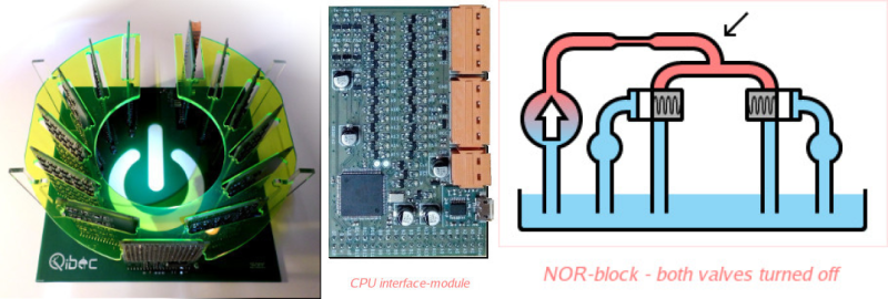
One additional module is a combined data-latch (8 transistors) and a 16×16 LED-display, at the front. Another module is an interface-bridge between the CPU’s address- and data-bus and a host-PC, acting as “serial RAM/ROM”. Both these modules were designed using traditional schematic capture and layout. The website doesn’t talk much about these modules, because they are not part of the CPU proper, and both will definitely change drastically.
I didn’t publish layout-files (Gerber) yet, since there are still some things unclear to me w.r.t. licensing.
There were no fanout-issues – to be honest, I guesstimated it would be OK using the given resistor-values, and just went with it :-) Propagation delay is a non-issue here, because there’s a deliberate pause between gating-signals for different subsystems being active.
I’ll be at Maker Faire Hannover, Eindhoven, and likely in Dortmund – perhaps I’ll see you there. BTW, Twitter #Qibec shows some more pictures of a working device. One thing you will notice is a hack-PCB being used on the timing-module, because that did not work at the time (pulse lengths too short, and flawed construction of AND- and OR-gates). Instead of investigating, I decided to concentrate effort on presenting a working system at Maker Faire.
So… it works, with a hack :-)
actually… come to think of it, the combined data-latch and LED-panel board were done using that same netlist-generation script.
Using such a script may be nice for circuits consisting of “many duplicated simple things”. Anything beyond that is a PITA, obviously.
If interested, you can read a bit more about the netlist-generator here http://home.mircad.nl/md/KiCad_without_Eeschema_or_CvPcb.html and here http://home.mircad.nl/md/KiCad_with_generated_net_and_cmp_files.html .
I am surprised there are licensing issues. Do you mean “What license should I release this under”, or “Am I legally allowed to release this”?
Anyways, as it stands, this CPU is pretty much unusable for its intended educational purpose, without schematics or a BOM.
I would like to allow use for non-commercial purposes, but disallow use for commercial purposes (Creative Commons BY-NC-SA license). The issue I’m not sure about, has to do with using a digital file (Gerber, say) to make something physical, bypassing the intended license. So I’d rather be safe than sorry, in that regard, until I gain clue in that area.
That said, I think the project is not finished, but at least presentable – you’re right, at this point not enough information is given to recreate it at home. But the idea should be clear, at least I hope it is. We’ll see how this develops.
Yeah would suck if the iPhone 12 had this CPU and you didn’t make a penny.
;-)
I think most programmers would get bored with this instruction set in a few seconds. Go to https://en.wikipedia.org/wiki/One_instruction_set_computer for some insight on turning-complete computers using only a single instruction. Apparently that’s a thing.
Not only it is a thing but it is a commercial product. Maxim integrated sell the MaxQ MCU which are single instruction set microcontroller. The main advantage is that those MCU generate less noise. The Q meaning Quiet.
https://www.maximintegrated.com/en/app-notes/index.mvp/id/3222
Last time I looked, though, Maxim didn’t promote the OISC nature of it. The assembler “hides” it by giving you opcodes that do what you want. My Asm for One-Der does the same thing, so I’m not saying it is a bad idea, but just that they don’t make a lot of fuss over it being one instruction.
Random links:
Early version of One-Der: http://www.drdobbs.com/embedded-systems/the-one-instruction-wonder/221800122
Cross assembler for One-Der: http://www.drdobbs.com/embedded-systems/a-universal-cross-assembler/222600279
(I also wrote about this for other CPUs here on HaD: https://hackaday.com/2015/08/06/hacking-a-universal-assembler/)
Forth for One-Der: http://www.drdobbs.com/architecture-and-design/the-commando-forth-compiler/222000477
OISC Textbook (not mine): http://www.caamp.info/
Lots of research on TTA: http://tce.cs.tut.fi/
Novel TTA “Microcode” patent (mine): https://www.google.com/patents/US9081582
This is not really true. Yes, the MAXQ architecture only has one instruction – a move instruction, but it has an addressable ALU, meaning that by moving data to a certain pair of addresses, you are causing a separate part of the CPU to execute an addition, or subtration, or logcial operation, which you get the result from by moving from the address of the result location for the ALU to somewhere else. So yeah, you COULD say it’s a single-instruction CPU, with a set of coprocessors, but that could be construed as misleading.
From Maxim’s description, the big advantage this provides is that by separating out various functions that would be performed by a logic array in a more conventional CPU, is that these “peripheral” (my quotes) processers can be effectively declocked when not in use, which results as you say in less generated noise. An interesting architecture – thank you for pointing it out.
I don’t think the first paragraph is appropriate at all, one instruction cpu is hardly a great primer, just begs more questions than it answers really.
Depend on the instructor/learner. In isolation, probably not. But I have used a different oisc with students successfully and there is any least one text book out there that is similar. The transistor gates might be more of an issue but, again, I think the right instructor could pull it off. Depends too on what you are trying to teach or learn.
I agree strongly.
Sorry Michai, I’m just not a fan.
Exactly why does “D” get to be called “data”? Isn’t it really just a half-rate clock? Couldn’t you just fetch and increment each cycle, and not even have the contrived datapath?
Apart from that, this hardware is at least a nice interesting piece of electronic art, but for ‘education’??
OISC’s are *terrible* as primers. They just ‘hide’ the complexity elsewhere. In this case, it’s in the code. Somewhat like Tupper’s self-referential formula.
Hardware that requires self-modifying code to do anything interesting/programmable fails heavily under the ‘too simple’ principle, as in “everything should be made as simple as possible, but no simpler”.
I feel sorry for anyone trying to understand computer hardware who meets this thing first!
It’d be like a teacher trying to introduce you to coding by **starting with brainf*&k** !
They should instead go read “But how do it know?!” by J. Clark Scott, and/or else buy an iceStick and follow the manual at .
Alternatively, there’s even a game now on steam greenlight : “Hardware Engineering”, which will teach anyone who persists at it exactly how computer hardware works.
The “D” is indeed for “data” (or I am misunderstanding you – “D” has nothing to do with a clock, except a derived clock is used to latch a data-bit, or enable the latch, yes). The building block you might refer to is a (gated) D-latch: https://en.wikipedia.org/wiki/Flip-flop_(electronics)#Gated_D_latch . I don’t understand your comment about “fetch and increment each cycle”.
My goal was to fill a gap between simple hardware (transistors in saturated/cutoff region used as switches) and a first program. To me, the project ends there. It wants to fill a niche. Furthermore, I don’t think a spartan instruction-set is an obstacle for most users; that’s why compilers exist. That area falls completely outside the scope of the project, as far as I’m concerned, although I did make (on paper) an imperative higher-level language for this CPU, just for fun.
You seem to be under the impression that self-modifying code is used, while in fact it is not – program-data in ROM is only being read, and data in RAM is non-executable. I think I agree with you that self-modifying code can be a nice puzzle, but it may stand in the way of getting the concept of a simple program across.
I’m not sure I agree completely that starting with BF is totally bad, BTW :-) Or with a Turing-machine, for that matter.
I didn’t look at related games, but did look (in retrospect) at various simple CPU-implementations. Some of these were emulated only. To me, something I can poke a DMM or scope at, makes a bigger impact than a PC-program (assuming you meant that). But tastes differ, of course.
Thanks for your feedback though – one of the reasons for posting here was to get diverse feedback.
actually, about your comment about “D” / “data”, can you tell me where you saw that (on the Qibec.org site)? If it’s unclear, perhaps the text needs to be changed.
Thank you all for the feedback, I appreciate it.
I made a video about the appearance of the device, its basic operation, the way it is programmed and future plans here: https://www.youtube.com/watch?v=ZCmbSl5–1Y . I hope this makes the material a bit more accessible. It also addresses some of the points that came up on this thread.
Thanks for this, Michai – it goes a lot further in explaining how this is useful, even though there was far too much “which I won’t explain here because it’s on the website”.
An important factor to me was seeing how you made this actually programmable, through the use of a macro assembler to basically synthesize instructions that are much easier to use. Ever since I first encountered the idea of single-instruction-set computers, I thought that they would be impossible to write any more than the most simple programs for, which explains my earlier comment about getting bored with it very quickly. But using macros makes this trivially easy (once you figure out how to implement more useful instructions), which DOES make a machine like this useful in an educational setting. In that respect, these macros serve kind-of-just-a-little-like microcode does in a microcoded CPU – the programmer doesn’t need to know what’s actually going on inside the CPU on a cycle-by-cycle basis, because this is abstracted out to instructions that are more code efficient and human-friendly.
I also agree with you about some of your comments toward the end of the video – it would be a lot more impressive as a stand-alone machine, on which you could download object code from your macro assembler and then disconnect. Also, writing a simulator for it would probably speed up the development process. And actually, having grown up in the 8-bit era (and earlier), to me it seems like designing and building the interface to connect it to the “host” PC was far more work that simply adding some RAM and (flash)ROM to it. And then, seeing that rather than debugging your timing board problems, you basically replaced it with a microcontroller tells me that you’re more comfortable with software than hardware. Which is fine – it adds more to the accomplishment of having built some hardware that you can now write software for.
Wasn’t sure what to do w.r.t. video length and content, really. This one is still about 30 minutes and doesn’t explain everything. Some people have suggested there be a (much) shorter video, which I’ll shoot tomorrow or something, as “even quicker tour” – about 5 minutes long.
I like the style of the “AltairClone” (Altair 8800 clone) YT videos a lot. Binge-watched them all, although I have no actual experience with that machine. Perhaps there will be bite-sized videos about the Qibec CPU too, each dealing with one specific concept, feature or issue. Videos take relatively little time to make – at least the quality I make them in :-)
Just recorded a 5(ish) minute long video: https://www.youtube.com/edit?o=U&video_id=UBlCEsLfgiI
And… just recorded another 5(ish) video showing a visual way of programming: https://www.youtube.com/watch?v=weeKqSuAEo4
(JQuery code to make a visual program-layout, which is then sent to a Ruby CGI-script, validating, assembling and running the resulting binary on the CPU.)
Obviously this has little to do with the CPU itself, and is more of a generic tool to show what a program can look like. Shown at a local event here, and well received by kids. Some of them then started to wonder “what was in the box with all the green boards”, so yay, another electronics/embedded engineer in the making :-)