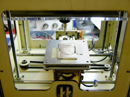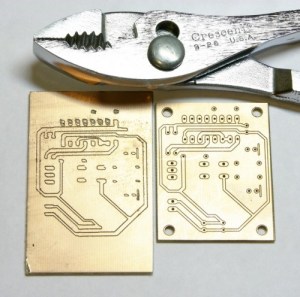
[Keith] wanted to use his makerbot for some PCB milling, but he ran into a pretty big problem. The platform that his PCB would sit on was mounted with a layer of double sided foam tape and was not perfectly aligned to the head. Not only that, but it would tilt when pressure was applied. This made the result of the milling completely unacceptable. To remedy this, he made a new platform that is not only rigid, but he has made it so that there is the ability to adjust it for perfect alignment via adjustment screws in the 4 corners. At the beginning of each session, he can be absolutely sure that everything is aligned perfectly and his PCBs show a huge improvement. You can see a comparison of the two in the following picture.

[via HackedGadgets]


so how does he drill? you need some soft material of at least 0.3 mm underneath the pcb.
If only the makerbot didn’t cost >1K…
Did you even read the article, Caleb?
“The results were not tremendously better than before (left board, top row of pads; right board from commercial mill for comparison)”
His results after improvements, are on the left.
I wouldn’t use that board! I wouldn’t use his mill.
We don’t get from Prototype to production by dismissing first attempts.
The Makerbot is one of those tools that will never be 100% of everything to 100% of Hackerdom. Don’t slag anything Hacked from/onto the MBI gear for it’s not being factory floor ready. Here’s why:
The term Rapid *PROTOTYPE* Tool is what needs to be applied properly.
So whatever we do with the MBI stuff is true Hacking as we’re using a tool originally designed for IIRC- Frosting Cupcakes to do so much ..MORE.
The other applicable term is Toolchain Creation.
Milling a PCB makes these ‘bots a step closer to more fully self-replicating every component. The steps from Concept Proof>Production are non-trivial but lest we forget why we do some things these ways?
**WE’RE HACKERS**
The results are impressive. Given that the makerbot isn’t designed to handle any cutting forces on the carriage. Not a bad way to bang out a prototype to make sure everything works before sending the design off for manufacturing. All in all a good hack.
Pretty nice show. However, I would propose to etch the PCBs, milled PCBs are slow, unprecise, expensive and only suitable for THT if you don’t have some really good mill. Makerbot only qualifies as cheese mill, I guess…
his results are pretty much what i would expect a cupcake to do to a pcb
building cheap machine hw is always going to be challenging, i think maybe he would benefit from either not using belt and pulley system, or adding some closed loop control element
also going to the effort of getting that plate made and then taping the pcb down is two steps forward and one back. at least its better than the foam
I wish highly-visible hacker blogs weren’t picking up my PCB milling experimentation mid-stream, as I hope to have something significantly better to show for my efforts one or two more stages down the line. Please allow me to address some misconceptions.
As already noted in the comments, the left PCB is the best milled by the CupCake so far; the right PCB is commercially milled. The PCB made by the CupCake is not usable and by no means do I represent it as such.
The vast majority of the huge remaining backlash in the mill is due to the plastic bushings on the X-Y stage’s guide rods. Thingiverse has a better design for a bearing-based guide system that has less play *and* that isn’t overconstrained. I plan to build it soon, as it will improve both my FDM and my PCB milling. That will be the point at which I decide whether the CupCake can produce PCBs good enough to use while prototyping.
This is not about building the best, or even a terribly good, PCB mill — it’s exploration whether the CupCake can support a different toolhead (milling) well enough to be worth using with the framework I (and others) already have. This is not at all how I’d go about building a mill from scratch.
Regarding etching PCBs — I have done so for over two decades and I don’t particularly enjoy it. The etching process has many stages at which things can go a little bit wrong; the milling process produces results with very little deviation. Once I have a satisfactory milling setup, I would much rather fire-and-forget with the mill than tend, tend, tend to the multi-step etching process.
Regarding drilling with this mill — I don’t think it takes a genius to figure out that I can mount a sacrificial MDF plate between the aluminum leveler and the PCB.
And regarding the tape, if you haven’t tried it, you’d be surprised at how well-constrained a PCB is with tape on opposite edges in two axes. The proof, if any is needed, is that the PCB made with the commercial mill was held down with tape in the same fashion.
I looked at that Makerbot thing when it came out. Wayyy too much money. Not that it isn’t worth it. It’s just too much money… For me anyway; and I would venture to guess for many.
A 3d plastic extruder with a milling head? Brilliant. Useable? not yet. Results are not unexpected. Taking something and making it do something else its not designed for? A true hack. Good job and with a bit of work and some more precise parts it may turn out some usable boards!
Cheers
Does anyone know the long term effects of breathing in fiberglass dust? I seem to recall it being up there on the same order of bad-for-you-ness as asbestos. I guess the kind of fiberglass in insulation isn’t great for you – but the chunks are big enough that if you get some in your lungs, your body will expel it. But if you make it into a dust, that when it’s the right size to stay and cause cancer….something like that anyways.
I never had the tilting problem – someone at the Fablab asked me about it, turns out you get that when you use only one piece of double-sided tape.
If you use two, no problemo.
–Nathan
Could the plastic emitted from the Makerbot in its “normal” function be used as a resist layer for etching a PCB? How precise is the extruded plastic being laid down?
Dosbomber, extruding plastic onto a PCB as etch resist is an interesting idea. nophead found that ABS sticks to warm copper but pops right off as it cools and PLA sticks well to warm copper and can be removed when cool by flexing the PCB.
http://hydraraptor.blogspot.com/2010/04/cu-pla.html
The MakerBot CupCake’s nozzle is .3mm (~12 mil) diameter, but the plastic experiences some die swell after exiting the nozzle and (more importantly) requires pressure to stick to the platform, deforming it into an oval or worse. I would estimate 16-mil traces would be the narrowest I could produce with my nozzle and 20-mil would be more likely.
That’s not bad, but I comfortably hand- or hot-plate-solder TQFP, TSSOP, etc. packages and when laying out boards occasionally reduce trace size to 12-mil in the vicinity of the IC. The commercial mill to which I have occasional access has no trouble producing usable 12-mil traces with 8-mil isolation, and these are *especially* the boards I’d like to be able to rapid-prototype at home.
One would likely want to use a finer nozzle (Thing-O-Matic? custom?).
Riddle me this: What do you do with an etchant-soaked PLA doily in the shape of a circuit once you’re done? I suppose throw it away.
nope, Caleb has not read the article he discusses here…