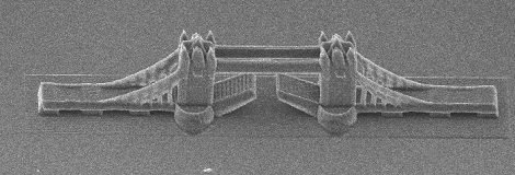
This 3D-printed model of the Tower Bridge is only 200 micrometers long. To put that into perspective, the distance between the towers is the width of a human hair. This model is the product of research at the additive manufacturing department of the Vienna University of Technology
The models were fabricated much like normal stereolithography – a laser shines onto a vat of light-sensitive resin. The resin hardens when exposed to light, and the model is built up layer by layer. These nanoscale models were made using a process called “two-photon lithography,” something we’re not going to pretend we understand completely but here’s a nice paper that provides a good overview. Needless to say, the precision these prints exhibit are nearly ludicrous. The researchers claim a precision of ±1µm, a respectable amount of precision for very high-tech machining applications.
The researches posted a video of the fabrication of a nanoscale F1 race car filmed in real-time. Check that out after the break.
[youtube=http://www.youtube.com/watch?v=5y0j191H0kY&w=470]


OMFG Awesome!
Slow right now but this blows anything else out of the water in terms of ultimate achievable quality and detail.
Just as an example, 15 micron layers are about the smallest you are going to get on commercial machines right now. This appears to be able to produce FEATURES at 1 micron or so – and thus layers at or below 1 micron. That’s a 15x improvement over the best, $100,000+ photopolymer machines on the market today from 3D Systems, Objet, etc.
Not sure how well you can produce objects that are unsupported (these examples are all flat) but just like SLA, I don’t see why you couldn’t also produce “break away” support surfaces.
Like any other technology. Baby steps first. This is absolutely incredible.
Who said nano-bots can’t be made?
micro, not nano.
nanometers would be smaler than the wave length of visible light. i’m sure there would be problems.
remember: dx * dp =< h/(4PI)
so much for my knowledge of physics.
i meant larger than, not smaller :D
Visible light may bottom out at around 380 nm, but there are other techniques available. Both UV and X-Ray lithography should be able to theoretically resolve to less to less than 50 nm. Granted, both present other major challenges, but I’m sure someone will figure out how to work some magic eventually :)
3D chips! Just one step closer to the SkyNet Apocalypse!
If I recall from the news I read, these require a scanning electron microscope to even image the final product.
Look up 2 photon microscopy for a good understanding of the principle.
It’s pretty sweet.
Up Next: Nanopr0n!
Size does matter!
NewF1CarMicroMicroMachinesFromMicroMachines!ItDrivesRoundTheTrackAtAlmostTheSpeedOfMyVoice! NewSubMiniManufacturingAllowsTheseNewMicroMachinesToBeEvenSmallerThanTheLastGeneration!SoSmallYouCan’tSeeItWithoutAMicroscope!SmallEnoughToGetLostInTheCarpet!You’llHaveABlastUntilYouOpenThePackage!
MicroMicroMachines…NewFromGaloob!
That is some very nice Micro-/Nano-Art. I once had the honor to be part of a japanese research team researching FIB-CVD which can do similar things. It is amazing that they managed to create abitrary structures, not using CVD but lithography. Thanks for the interesting read!
So if they can 3D objects made out of metal such as titanium and can now make objects this small, can they made want could in theory be the world’s sharpest knife? Very cool!
Wayne, that would be pretty hard to beat since the absolute sharpest knives out there would be something like obsidian surgical blades. The cutting edge on those can reach down to about 3nm thick.
These machines are sweet. We got one at our school about a year ago and they can do amazing things. Sure they’re slow and somewhat tedious to set up (the photoresist gets pricey too) but can make amazing structures in the right hands.
So, they literally can make the worlds smallest violin and play a sad song on it.