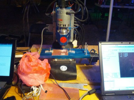
[Hao] from Noisebridge showed me their CNC mill being used to etch PCBs. Using copper clad board, this MAXNC 10 mill routes the PCB with decent accuracy. This makes for very rapid prototyping of single sided PCBs.
[Hao] designed the PCB using the open source KiCad EDA tool. This was used to draw the schematic, layout the PCB, and generate the Gerber files. Next, pcb2gcode was used to convert the Gerbers to G-code, which is a standard set of instructions for controlling CNC devices. Finally, LinuxCNC was used to send the G-code instructions to the mill. It’s a powerful application of a completely open source workflow.
The PCB being milled is for a pressure based touch sensor. It uses the Freescale MPL115A barometric pressure sensor encased in a rubber housing. This sensor is being incorporated into the Dora Opensource Robot Assistant project, which [Hao] and the Noisebridge folks are working on. We’re looking forward to hearing more about the Dora project in the future.


The title is misleading. He is doing board layout in kicad, but he is not using it to mill the PCBs. The g-code generation and milling operation has nothing to do with the layout software, once gerbers are made the program used becomes irrelevant…
Agreed.
Also on a side-note: If it’s not an elephant it’s irrelephant. :P
It’s not irrelevant to the fact that “It’s a powerful application of a completely open source workflow.”
That mill looks really interesting, any info on it?
I am interested in the mill as well, was it homebuilt or is it commercially available?
http://www.maxnc.net
In general it’s no good idea to mill PCBs. Either shitty resolution or huge cost in burr tips (small ones wear out quickly). Also the traces are not rectangular in cross section but trapezoid, triangular in the worst case, hindering soldering and reducing allowable current.
The guy who made the blue laser printer to directly expose the layout on a photosensitized board is definitely onto something much more practical and useful.
Anyone else have comments on this? I’m currently finishing a pcb milling machine, and these concerns are new to me.
I’m not sure why a slight trapezoidal shape to the copper traces would matter. When etching you get some undercutting that does the same thing. Sure mills wear out, but so do drills, and for through hole boards even if you etch you gotta use drills.
I have to agree that milling PCB is not best solution. I bought MAXNC for milling boards, but now I use it only to drill holes. And it is good for that. Cutter bit wear, bad resolution, slow, short circuits to other side of cut and varying cut depth were my problems. The last was caused by PCB that tend to bend when attached. Currently using photo sensitive PCB for high resolution (0.5mm trace) and toner transfer for low resolution (>=0.8mm trace).
Engraving tips work much better and cleaner.
I’m hoping to try some board milling with my ShapeOko when I get it up and running. I stumbled across pcb2gcode just this morning, what a coincidence :-)
Why stay single sided ? You just have drill 4 holes with the cnc in the pcb and in a piece of plywood. Put some rodes in the plywood’s hole, use them to align the pcb, mill, reverse the pcb. Perfect alignement guaranteed…
Another way for double sided boards is to just flip it over after the first side is done and use a webcam mounted on the mill to discover the location of the pcb. Using camera’s for this is standard practice in smd placement machines (feducials etc). and it has also been done by hobbyists. I even believe a worked out example was here on hackaday a few months ago.
I’ve got a similar (yet completely different) setup – using Eagle, pcb-gcode, Mach3 and a converted Proxxon MF70 mill. I’ve used it to mill some through hole and surface mount stuff – the smallest being SOIC so far.
The thing I’ve found hardest is fixing the PCB completely flat. Clamping as in the picture tends to make the PCB bow up in the centre. This causes deeper cuts, and if you’re using a V bit it can also cause chatter and a ragged edge. (A 0.5mm end mill avoid the chatter due to the straight sides.) I’m considering a small vacuum table.
If anyone has useful info on effective hold-down that would be a great.
If you have measure probe you could measure PCB heights and make compensation to G-code. Here is my project about that: http://www.rouvali.com/index.php?id=55. Please note that reading digital micrometer with webcam is not something you want to do :-) But I hope you got the idea…
Thanks. I may look at some sort of probe solution but that seems like overkill when you’re just trying to get a flat board to lie flat on a flat surface!
Overall though I have to say I’m a fan of milled boards. No chemicals and perfect alignment for drilling and cutting out the board on the same machine.
I am more toner transfer/photoresist guy now, as I wrote up there some were. It all depends on what you are doing and with what tools you have.
Oh, one more tip: Paint your PCB before milling. If you cut too thin at least you remove some paint and board can be fixed with chemical etching.
what make is this benchtop cnc mill
this really intresting!