[Gene] has a project that writes a lot of settings to a PIC microcontroller’s Flash memory. Flash has limited read/erase cycles, and although the obvious problem can be mitigated with error correction codes, it’s a good idea to figure out how Flash fails before picking a certain ECC. This now became a problem of banging on PICs until they puked, and mapping out the failure pattern of the Flash memory in these chips.
The chip on the chopping block for this experiment was a PIC32MX150, with 128K of NOR Flash and 3K of extra Flash for a bootloader. There’s hardware support for erasing all the Flash, erasing one page, programming one row, and programming one word. Because [Gene] expected one bit to work after it had failed and vice versa, the testing protocol used RAM buffers to compare the last state and new state for each bit tested in the Flash. 2K of RAM was tested at a time, with a total of 16K of Flash testable. The code basically cycles through a loop that erases all the pages (should set all bits to ‘1’), read the pages to check if all bits were ‘1’, writes ‘0’ to all pages, and reads pages to check if all bits were ‘0’. The output of the test was a 4.6 GB text file that looked something like this:
Pass 723466, frame 0, offset 00000000, time 908b5feb, errors 824483
ERROR: (E) offset 0000001E read FFFFFFFB desired FFFFFF7B.
ERROR: (E) offset 00000046 read FFFFFFFF desired 7FFFFFFF.
ERROR: (E) offset 00000084 read EFFFFFFF desired FFFFFFFF.
ERROR: (E) offset 0000008E read FFEFFFFF desired FFFFFFFF.
ERROR: (E) offset 000000B7 read FFFFFFDF desired FFFFFFFF.
ERROR: (E) offset 000000C4 read FFFBFFFF desired FFFFFFFF.
ERROR: (E) offset 000001B8 read FF7FFFFF desired 7F7FFFFF.
ERROR: (E) offset 000001BE read 7FFFFFFF desired FFFFFFFF.
ERROR: (E) offset 000001D2 read FFFFFF7F desired FFFFFFFF.
Pass 723467, frame 0, offset 00000000, time 90aea31f, errors 824492
ERROR: (E) offset 00000046 read 7FFFFFFF desired FFFFFFFF.
The hypothesis tested in this experiment was, “each bit is independently likely to fail, with exponential dependence on number of erase/write cycles”. There were a number of interesting observations that led [Gene] to reject this hypothesis: There were millions of instances where an erase did not reset a bit to ‘1’, but none where a write did not change a ‘1’ bit to ‘0’. That’s great for developing an error correction code scheme.
There was also a bias in which bits in a word produced errors – bits 31 and 32 were slightly more likely to have an error versus other bits in a word. The most inexplicable finding was a bias in the number of failures per row:
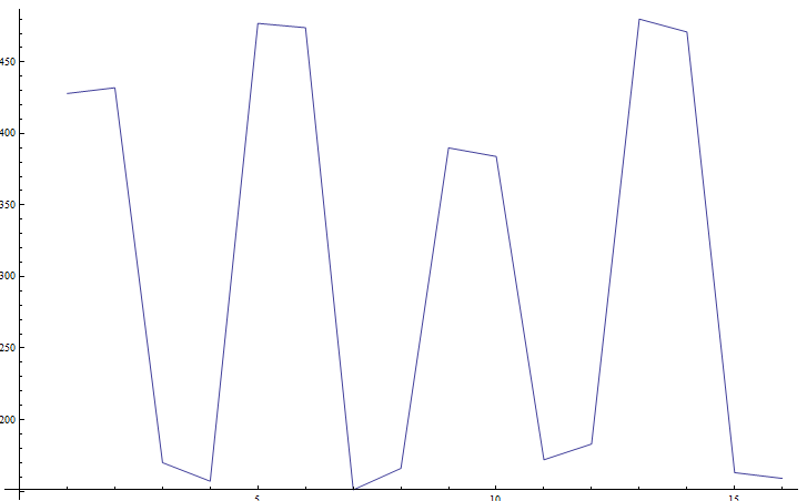
A row of Flash in a PIC is 128 bytes, and if all rows were equally likely to produce an error, the above graph would be a little more boring. It’s odd, [Gene] has no idea how to interpret that data, and only decapping one of these PIC and looking at it with a microscope will tell anyone why this is the case.
At the very least, Microchip is severely underrating the number of Flash read/erase cycles on this microcontroller; this chip was rated for 20,000 cycles, and the very first failed bit happened on cycle 229,038. With a separate run, the first failure was around cycle 400,000.


Of course they severely underrated the number of cycles – it is dependent on the fabrication process and operating temperature, both of which can negatively impact the memory’s lifetime.
So when these devices say “field programmable” they really mean “not field programmable”
What? No, they are still field programmable. They just don’t rate them to more than 20K write cycles.
It just mean the part can be reprogrammed without you having to send it back the factory to pull out the chip onto a special programmer to reprogram it.
The keywords are field and programmable. There is no implied meaning of it being reprogrammable for *infinite* number of cycles.
From the archives: testing the EEPROM on an AVR chip.
http://hackaday.com/2011/05/16/destroying-an-arduinos-eeprom
“At the very least, Microchip is severely underrating the number of Flash read/erase cycles on this microcontroller; ”
Probably not. They will rate them for to operate reliably over the range of voltages and temperatures allowed by the device datasheet, as well as other aspects of the flash wear mechanisms that only the chip designers may be aware of including address and data pattern sensitivity. They almost certainly then add safety margins to allow for the spread of device characteristics across multiple wafers. These factors could make a huge difference between the data sheet cycle limits and those found in the testing described in the article.
“other aspects of the flash wear mechanisms that only the chip designers may be aware of”
Are you saying they leave these details out of the specifications for some sadistic reason? “hahaha let the customers moan and complain about short flash life, this is fun, let’s leave more data out of the spec sheet next time and see how they squirm”
No, of course not.. I specifically said “including address and data pattern sensitivity”.
For example. the layout of the silicon may mean that specific combinations of data and addresses may result in marginally reduced or elevated voltages within parts of the chip which can affect how well it performs. There is nothing unusual about this in semiconductor memory devices, but there’s nothing unusual about not putting it in device data sheets either. The data sheet presents a set of conditions under which the manufacturer guarantees the chip to work. You never need to know about the small percentage of conditions that get much closer to that limit than any others, since it would be nearly useless information for most hardware and software designers.
Moreover, say the dependence of the fault rate on the second bit of the row address may mean that they have an “easy fix” for this. This is something they can test in production: the original “slightly worse” performance of A1=0 rows might be due to a voltage droop in the internal VCC net. So beefing up that wire should improve performance. If they do that “in production” they have an easy and cheap supply of chips to test this theory on. Then for a new generation of chips they might include the improved layout AND the better specs.
Microchip isn’t underrating something – they just say that it will survive 20.000 E/W cycles and it indeed does :-)
Apart from that, test seems to be done at room temperature. Running the test at elevated temperature would bring failure sooner.
The one worry I would have here is that not only does flash develop bit errors after repeated erase/write cycles, its data retention lifetime drops.
After you’ve erased/written data for like, 100,000 times, that data might fade in a year or so, especially if it’s in a hotter area. Obviously you can’t test that on a bit-level basis except at really high temperatures and over a very long time, so it’s pretty neat to see the bit-by-bit structure for failure – but even if the bits haven’t “failed” , there’s no guarantee that they’ll retain their data long-term.
I would think that block erase and the individual write operation would likely cause the most stress in the FLASH cells due to high electrical field. What is likely to happen is that the cell would be more leaky initially (i.e. may start to require longer erase time and cannot retain data as long) and eventually would fail on those erase/write operations. Hard failures are easier to deal with because you will know right away, but retention types are going to be an issue.
Regular ECC are typically for dealing with single bits or multiple bits is not going to be efficient if there are wide spread errors in a localized block (vs spreading the redundancy globally). You can detect and correct early retention errors by scanning the memory regularly, but that’s going to have lots of overhead. Might be better off to set aside blocks for using something like par2/par3 type of recovery that works at block level. Also you would have to have some spares too for relocating blocks. Can you application handle the wait for the recovery?
There is also the option of using off-chip storage that are optimized for erase/write cycles. Some of the older EEPROM are rated for 1M (or more?) cycles. If they should fail, you can replace that part.
What about retrying the erase command? Would that work? I remember in the old times of UVEPROMS the recommended programming algorithm involved programming multiple times until it verified, and then programming some more. It would be interesting to see if a block that fails to erase can actually be erased by repeating the command
You probably shouldn’t want a block that fails a erase even if it works the 2nd try if it has worn out to that extend. Better off to use a different block instead if you care about your data.
If one tries this with an SD-card, does the card have write leveling feature or is it direct like this situation?
The SD card deals with the wear leveling internally (sort of like you expect in a SSD).
Think on board 8051/8052 processor and an array of write counters (stored on slightly longer life flash) , to track block usage and migrate data to keep wear level.
Someone decapped a PIC32MX340: http://siliconpr0n.org/archive/doku.php?id=azonenberg:microchip:pic32mx340f512h
“A row of Flash in a PIC is 128 bytes.”
Correction: A row of Flash in *this* PIC is 128 bytes. Not all MCUs use the same type of Flash. For instance, I’m working on a project now that writes its non-volatile settings to Flash on a 16F1613 (enhanced midrange core). In this case rows are 16 bytes and Microchip only guarantees an endurance of 10K erase cycles.
“Wear leveling” in NAND is good for a bunch of reasons, but ECC can be still valuable even with wear leveling. Since the bit errors are sparse and non-bursty, a short convolutional code seems well suited.
Flash endurance is a fade problem. Every time you reset the gate, you reset the data expiration date. And every time you do that, the expiration date gets shorter. The 20,000 endurance spec is usually rated such that at a 20,000 accumulated erase count, data is guaranteed to be retained for a period (typically one year) at a given temperature specification.
When verifying flash endurance, testers typically use an Arrhenious equivalency to accelerate testing time for a given temperature rather than running up the erase count and waiting months or even years.
The random pattern you see is most likely variance in the silicon wafer from which the flash part was etched.