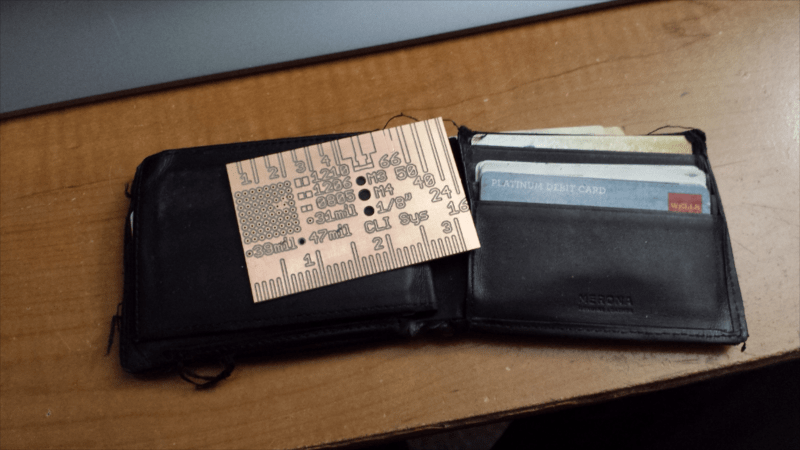
Hobby CNC mills have made rapid prototyping easier and faster for hackers. One really useful application is quickly fabricating your own milled PCB’s. [proto logical] built a Reference PCB Business Card using his CNC mill after repeatedly coming across other hackers who were not too convinced about the capabilities of CNC mills in routing PCB’s (also referred to as isolation milling). He thought of making a business card sized reference PCB to show around when he bumps into such folks.
To keep it useful, he included inch and centimetre scales, 0.1″ grid of holes, reference track widths from 16 mil to 66 mil, a few common drill holes and vias and some SMD foot prints. The single sided board is 50 mil thick, so it doesn’t bulk up his wallet. He’s posted the Eagle board file (direct download) and G-code (text file) for those interested in milling their own reference boards. The idea isn’t new – it’s been tried several times in different form factors in the past, generally using more traditional techniques. [proto logical] got inspiration from [Rohit Gupta’s] TinkerRule – The Maker’s Swiss Army Knife. Then there’s the very popular uRuler made by [Dave Jones] of EEVBlog fame. If you have any suggestions on improving the design, chime in with comments here.
Thanks to [ACG] for sending in this tip that he dug up while looking for CNC routed PCB’s.


Too bad that the milling was fsckd up at the 66 and in the “veroboard” hole matrix…. If I was to use a pcb as a showcase for how good pcb milling can be I’d make sure it’s 100% properly done.
Showcasing the “realistic” expectations maybe? These aren’t too hard to fix by hand,
“using his CNC mill after repeatedly coming across other hackers who were not too convinced about the capabilities of CNC mills”
Maybe… But I can only interpret that quote from the HAD text that he thinks the method is good and the people he meets are a bit on the sceptical side.
Anyways, I’d love to have one of those 3040 CNC’s in my lab…
That is not even high resolution what you can achieve with 3040 or 6040.
Here’s my attempt with my 6040: http://tulos.tuu.fi/?p=299 – the pads are for Atmega 328p processor. And that’s not even the highest resolution that you can achieve. However with smaller accuracy you need to have the PCB really leveled, otherwise you might get cutted or unseparated traces.
See this article. compensates for non level surfaces. I have used it for PCB etching with much success. I find that many of the boards I buy are out by just enough for even a level surface engraving process to be insufficient. The G code ripper does a great job.
http://hackaday.com/2014/07/31/milling-curved-objects-with-a-g-code-ripper/
Meh, I easily do 100um traces with toner transfer method.
The things I found difficult when milling PCBs were not thin traces but closely spaced traces. Also, when applying dry film solder mask the deeper contours meant it didn’t work as well. Stick a TSSOP or LQFP with tracks running to adjacent pins on there if you want to prove what’s possible.
The big plus I found with isolation routing was perfect alignment with any holes or milling that you do.
Neat!
I had just designed a new business card in the same vein
https://mrrobot.ca/making-a-pcb-business-card/
It’s cool, though a good board house is so inexpensive these days that I’ve found it hard to justify getting a machine just to do more work and deal with more fuss just to get it done a week sooner.