This year’s DEF CON badge is electronic, and there was much celebrating. This year’s DEF CON badge has an x86 processor, and there was much confusion.
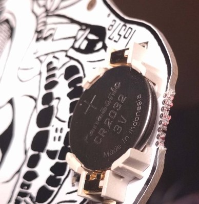
The badge this year, and every year, except badges for 18, 17, 16, 15, and 14, designed by [Joe Grand], and badges from pre-history designed by [Dark Tangent] and [Ping], was designed by [1057], and is built around an x86 processor. Specifically, this badge features an Intel Quark D2000 microcontroller, a microcontroller running at 32MHz, with 32kB of Flash and 8kB of RAM. Yes, an x86 badge, but I think an AT motherboard badge would better fulfill that requirement.
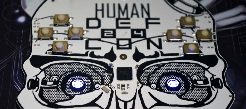
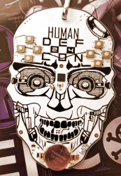
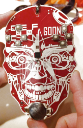
As far as buttons, sensors, peripherals, and LEDs go, this badge is exceptionally minimal. There are eight buttons, laid out as two directional pads, five LEDs, and a battery. There’s not much here, but with a close inspection of the ‘chin’ area of the badge, you can see how this badge was programmed.
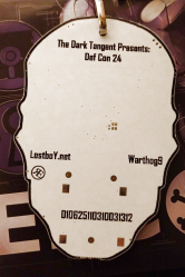
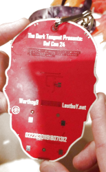
As with any [1057] joint, this badge features puzzles galore. One of these puzzles is exceptionally hard to photograph as it is in the bottom copper layer. It reads, “nonpareil bimil: Icnwc lsrbcx kc htr-yudnv ifz xdgm yduxnw yc iisto-cypzk”. Another bottom copper text reads, “10000100001 ΣA120215”. Get crackin’.
A gallery of the Human and Goon badges follows, click through for the best resolution we have.
This post has been updated to correct the record of who designed badges for previous cons.



I have an interest into hacking honestly don’t know where to start from this web site
teh pr0bl3m ist thou arntest typink enough k’s where g’s should be and 3’s where e’s should be… you’ll figure it out, eventually.
Ollydebug
Dsassm02
Hackaday doesn’t teach very much about programming or hacking into something like this, the main focus is to show off cool projects. To see more on how things are made check out hackaday.io which is where user made projects are. Those creators might be able to answer some questions about their projects.
Online tutorials are how I get through any project, and I studied engineering! Don’t give up!
Watch MacGyver, Mythbusters, and Star Trek (TOS).
Then take an unwanted printer or computer apart and try to figure out how it works.
you’ll never get anywhere, not because you don’t know where to start- but because your very statement shows you don’t have enough interest to start taking things apart, breaking them, figuring out how they work, fixing them, or better- mashing parts together to create something else entirely- and learning from those experiences.
+++++1
https://www.youtube.com/watch?v=S-H_cvcyKoY
Every one needs to start somewhere.
http://www.irongeek.com/
This isn’t the sort of hacking where you break into people’s computers with green text. It’s the MIT sense of “hack”, to mess around with things, to customise things and bend them to your will, to make things do stuff they weren’t intended to. More like inventing, than what the media call “hacking”.
Think you might be on the wrong site, mate.
If you wanna make a start on this kind of hacking, get an Arduino tutorial kit, and play around with that, that’s very rewarding and not too difficult for a beginner.
Despite the many other opinions on it, Arduinos are good for electronics beginners to learn from.
Pretty sure by “hacking” you mean computer hacking…this is not the site for that. Try elsewhere.
y’all are assholes
You can do anything you set out to do; don’t let negative comments influence you. Who are giving you the negative comments?–all those jerks [Bob Ross] directed his comment at; anyone who tells you you can’t do it; anyone who makes fun of you.
You’ve received some really good advice from many people here. Read as much of Hackaday as you can; you’ll probably find that you need to go elsewhere for more detail.
Meditate to the sound of 2600hz grasshopper.
While it might not be an AT motherboard, the CR2032 coin cell is bringing back plenty of (bad) memories… :-D
I still get night terrors after surviving the Throwie War of ’09
Wait, forgot where I was, I mean, but a raspberrypi zero and attach a USB hub, power switch and battery to it. Instant hacker.
Those vias look like somebody attempted to do mouse bites but accidentally put inner and outer copper on the holes.
Yes, 1057 designs the defcon badges every year.
http://www.grandideastudio.com/wp-content/uploads/dc18_bdg_slides.pdf
http://makezine.com/2009/08/02/kingpins-defcon-17-badge/
http://mirror.nitrous.io/defcon/defcon16-cd/Kingpin-Making_The_Defcon_16_Badge/defcon-16-kingpin.pdf
https://www.defcon.org/images/defcon-15/dc15-presentations/dc-15-grand-ode_to_defcon_badge.pdf
http://www.grandideastudio.com/defcon-14-badge/
But seriously, both 1057 and Kingpin have done an excellent job ;-). Not to mention the folks who make the paper badges when the electronic ones inevitably run out.
I guarantee someone’s going to ask if it could be running windows. I guarantee it.
Can you run Windows on it? LOL
Any processor can run any OS if you’re brave enough
http://hackaday.com/2012/03/28/building-the-worst-linux-pc-ever/
https://www.youtube.com/watch?v=tX2bZy4tXZE
Could it be running Windows?
There!
I rather ask “Why a x86 microcontroller?”
The x86 is the least platform i would expect in a micro, but at least with only 32/8 you don’t need to mingle with segment and offset too much, if you don’t go into protected mode as a first step anyway and leave realmode to rot. ;)
More security types know x86 assembly language than know ARM/Propeller/whatevers?
Thats actually a very good point. Once those server ARMs are competitive, that might change though…
I think you are right! ARM certainly are taking the cpu world by storm these days.
A quick glance at the docs in the link look pretty good and this may be a key reason for giving the Quark a try. I suspect Intel also offered sponsorship.But I wonder if the lack of much beyond the buttons is because of the BOM cost. 1057 may have also seen Intel’s claim about excellent security as a reason to get the Quark in the hands of hackers with a challenge to meet.
Reading about puzzles form previous years, these things take some crazy knowledge of crypto and cyphers as well as lateral thinking.
As for the Quark on the badge, maybe pairing one with an ESP8266 might result in some interesting hacks. I’ll be curious to see what comes out of Defcon this year.
Intel’s pricing isn’t competitive with what’s on the market. There are few migration paths – just small, medium and extra large. There are no advantages for it being x86.
I don’t want to know how much their hardware debugger/programmer would cost. Now if only they would release the specs and have open source debugger support.
True I cannot see why I’d use Quark over an Arm or even a MSP-430.
Have you checked out the link to the Intel page and browsed through the Quark documents?
Those specs you ask for are there. The Quark looks like an MCU, not a PC.
Their flash instructions involve a standard JTAG interface using OpenOCD. The bootrom looks like it’s open source.
This is not a PC that requires either Intel’s ITP or Assest’s sourcepoint debugger connected to an XDP3 port for debugging a Dediprog to flash the platform SPI ROM. This isn’t a PC CRB where you sign NDAs and get a reference flash image or go talk to an IBV to get platform firmware. this doesn’t look a thing like PC development. It may be the x86 ISA, but it is not an x86 PC platform. The Quark != a PC platform.
My question would be if the tool chain is that much better than working with other MCUs. They already mention using OpenOCD, the build documents mention make. If that’s GNU make, then perhaps GCC is also they recommended compiler. A flexible, mature tool chain that gives the developer a range of IDEs to develop in actually seems like a good thing. Do the free tools couples with the higher cost of the MCU offset the low cost of other MCUs couples with licencing a development environment such as Keil’s tools or RVDS? Probably not for an established developer.
I was gonna say the same thing, why do they even make that chip? X86’s horrible instruction set and trillions of transistors, but it doesn’t run PC software, the one thing that has sold every X86 of the last 30 years. Who’d want it?
Don’t security types use high-level languages like everyone else? Or C, ha ha ha!
Actually… could you run BASICA with 8K and 32K?
Probably not, since you’d need all the BIOS hooks.
@Chango
True you would have to some how hack up a bios for it but then if all your going to do is run a vintage basic there are 8052 and Z80 single chip controllers that would be better suited.
Yeah but how big was the BIOS? That was on the ROM too, quite probably the same ROM as BASICA. Would 32K do it?
I don’t particularly wanna run it, out of all the old BASICs there are much better ones from around the same time. Just curious if that’s the one bit of IBM PC software you could run on this chip. If you rigged up a CGA card and a keyboard and all that sort of thing. An ISA bus through the GPIOs.
Just an intellectual exercise, it wouldn’t be worth actually doing. Though you could also hang RAM off the ISA bus.
I doubt they put in the similar amount of transistors as their atom line of CPU as this is around 1/4 the price (which is still expensive). This chip doesn’t even have cache which is where a lot of the extra transistors ended up.
Had something like this showed up back in early 2000, they might have a hot product.
With most stuff being high level language there’s not much reason for embedded X86 anymore.
On the high end there’s Arm,MIPS,and PowerPC and on the low end there’s Atmels,MPS, and eZ80s
Fair enough it doesn’t have the cache, but I don’t imagine them designing it from scratch, I’d imagine it’s mostly the same die pattern as the central bit of whichever Pentium it’s based on. So it’s still got all the complex x86 stuff and it’s horrible heritage. Compared to, say, an ARM, which was designed from the start to be simple and efficient. Or a micro that’s designed for it’s intended purpose.
My impression is that this chip is basically a PC CPU core, but that since they got the process efficient enough to run at 3.5GHz without melting through your desk, the side-effect is that at low MHz it uses little enough power that they can call it an embedded chip.
I could be wrong. But x86 design is horrendously expensive, it doesn’t make sense to design one from scratch for embedded use, when there’s already many better chips for that use.
As for it’s price, that’s whatever they think the customer will pay.
When you’ve got the code, the bugs are in C. When all you’ve got is the machine code / firmware, all the bugs are in assembly language.
For the badge, I imagine they chose this to throw people into x86 assembly, people who might not be familiar with it already or who wouldn’t be interested/motivated/gimmicked-into otherwise.
As for why the D2000 exists in general, I bet it is to snag bigger fish than makers… if you have devs making phones and laptops and routers using x86… why not offer something familiar and to go along with the support relationships they’ve already established.
Also, if they focus on making it maker-friendly from a community and platform perspective, being the behemoth that they are, they can simply jazz up some better silicon with whatever IP blocks are most requested. It is a catch-22 though, they won’t spin new awesome silicon if makers/big-fish don’t adopt, but how do you reel in those customers without first having something snazzy? In this case I think it is brand-recognition, power efficiency being pretty good, and the high chance that they’re going to offer the-next-best-thing as soon as you get bored of the D2000 or Arduino 101. They’re thinking long-term too… building trust in the brand and maybe inspiring future-engineers.
Dos and Win 1? Why not. (Hey you never said which Windows!)
Never mind the architecture, those are some seriously cool and badass PCBs!
One thing I found interesting from a hardware level were the 9 solder jumpers that were on there. 1 for each of the switches and one on the upper-right forehead. I jumpered the left side, then all. It brings it into interesting new flash modes. You don’t have to know a ton about hardware/software reversing just to mess with it and have fun. Very much in the inclusive spirit of DEFCON.
At def con. We pulled the memory on first night and got the code converted into strings (had wire the jtag with copper wire through the holes and plier twists, didn’t have a good enough soldering iron). The boot screen on the vendor badge is a skull. Check reddit and twitter for more.
Would love to meet hackaday. You guys around at con?
JTAG through the ripped off header on the chin?
Any chance you could post the firmware ida dump to pastebin and reply a link? The stuff posted in the reddit comments (http://pastebin.com/9TwQeU5J) is incomplete as it does not reference any uart registers nor does it reference the rot24 strings. The through holes on mine are almost completely ripped off.
konami code