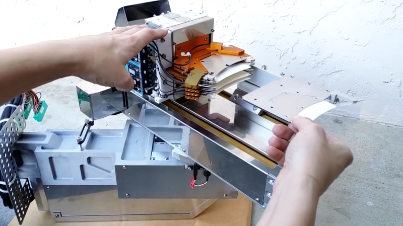
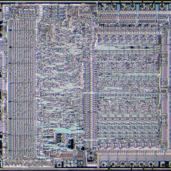
There’s nothing more freeing than to be an engineer with no perceptible budget in sight. [BrendaEM] walks us through a teardown of a machine that was designed under just such a lack of constraint. It sat inside of a big box whose job was to take silicon wafers in on one side and spit out integrated circuits on the other.
[BrendaEM] never really divulges how she got her hands on something so expensive that the engineer could specify “tiny optical fiber prisms on the end of a precision sintered metal post” as an interrupt solution for the wafer. However, we’re glad she did.
The machine features lots of things you would expect; pricey ultra precise motors, silky smooth linear motion systems, etcetera. At one point she turns on a gripper movement, the sound of it moving can be adequately described as poetic.
It also gives an unexpected view into how challenging it is to produce the silicon we rely on daily at the ridiculously affordable price we’ve come to expect. Everything from the ceramic plates and jaws that can handle the heat of the silicon right out of the oven to the obvious cleanliness of even this heavily used unit.
It’s a rare look into an expensive world most of us peasants aren’t invited to. Video after the break.


Fun video (I subscribed), and impressive piece of equipment, but I doubt that there’s any grand mystery in where BrendaEM obtained it… Surplus auctions can be amazing! For example, here’s a 5-axis manipulator robot that was used to move medical samples between test equipment. Bought it at a surplus auction … for $15 US !!
https://pbs.twimg.com/media/Cql7ks5VIAEgVOL.jpg
Sometimes it’s a good thing that i don’t have space at home i think…
You and me both…but oh the fun we’d have.
Buying stuff like this is a self-limiting game. There’s a *reason* I don’t have room for stuff like this anymore.
Looks like a fairly mundane industrial robot to me, I would not go so far as to say that the engineers didn’t have any budget–just that they were asked to build a robot that is absolutely going to work for the lowest total cost of parts+engineering hours. Things like having an alumina tray to hold the wafers may be expensive, but required for the machine to work reliably. Things like using a commercially packaged right angle breakbeam sensors where a simple LED and photodiode would have worked saves a lot of engineering time, since instead of wasting their time designing a reliable breakbeam sensor (designing the electronic circuity to be able to reject stray light, setting the thresholds, designing the mounting arrangement, etc as is required for an absolutely reliable sensor) they can buy one for a few hundred bucks and focus on engineering the parts of the system that can’t be bought from a catalog.
Spending on reliability on fab equipment pays off in the long run. A quick search puts a 12″ blank wafer at $500. Every step along the line the value increases, so at a minimum a single smashed wafer costs at least $500 not including the line downtime, cost to clean up the broken wafer, and cost for repairing or replacing the handler.
That’s peanuts compared to the cost of shutting down a line. Fabs have very expensive solutions to predict equipment failure before it happens so maintenance can be scheduled before things break.
Yeah, there is nothing special about the construction of this machine. I have taken a lot of old semiconductor process equipment apart and this unit is pretty par for the course. Definitely Japanese made from the parts used, maybe Tokyo Electron.
Alumina is used because it does not wear and leave particles behind in the system. Nothing to do with hot “discs”. Wafers…
The aluminum plates were almost definitely water jet machined. A laser table would have too much absorption in the material and would not only warp it, but would not be able to produce lines that fine in that thick of material without risking a high rate of rejection when manufacturing the specific parts. Aluminum would thermally conduct during laser machining and because of that, more material than was desired would either melt or enter a plastic state, risking severe defects in the parts.
The slits look more EDM than water jet cut to me.
No, it’s saw cut. Slitting saw on on arbor, they are not going to use a separate machine to just make some clamp slots.
You do make a valid statement for why the Aluminium isn’t laser cut.
But you forgot to mention that Aluminium is a rather good mirror for most types of light. As even a brushed aluminium surface will still diffusely reflect light, might not be a mirror finish, but it still reflects.
And Aluminium is a good substitute for silver in cheaper optical equipment.
Silver is almost never used in optical equipment. It tarnishes and enhanced aluminum coatings way outperform silver for the vast majority of applications.
Yes, Aluminium outperforms Silver in a lot of applications, mostly due to the vast price difference.
And yes, silver do oxidize rather fast, but so does aluminium, and both metals aren’t having good optical properties in their oxidized states.
In ultraviolet applications, aluminium is a far better mirror then silver, but the statement is though revers for infrared light however.
And in applications were low loss is crucial, for an example a CO2 laser cutter, then using silver would be a better option, as it has less then half the absorption at 940nm-1060nm, where most of the effective power of the laser in that case would be centered at.
Then silver is an effective band stop filter for roughly 320nm, as it absorbs almost all light at this wavelength.
But still, if you need something cheap, or broad band, then Aluminium is a really good metal.
CO2 lasers operate at 10600nm. Most mirrors for CO2 lasers are either just polished copper or a gold plated substrate like silicon, copper, or moly. Some cheap mirrors for low power CO2 lasers use a glass substrate.
Yag and other Nd doped lasers operate in the 1060-1064nm range. If you are using one of these lasers you dont use silvered or aluminum mirrors, you use dielectric mirrors. Same thing with other laser wavelengths like 2HG (532nm) and 3HG (355NM). These lasers are almost always Q-switched so they need the high peak power capability of dielectric coated mirrors.
Now seeing that I forgot a 0 in the CO2 Laser wavelengths. It should be 9400-10600nm.
Aluminum is laser cut all the time. We used to do it at the shop I worked at. But these parts are just saw cut.
THAT is the kind of thing to bring back from a Shenzen trip in the refurb market. Not gadgets that one can find on Alibay !
+1
Me, myself and I are going to Shenzhen next year. Do you know where I can find such markets?
THIS! I went there earlier this year for work (Mandarin speaking EE is a good combo) and I took half a day to walk around the markets (I think my watch logged something like 12 miles of walking, I was a wreck afterward) but I couldn’t find cool old, used, vintage, or refurbished stuff, which was what I was most interested in. If someone knows where to look, please share!
There is some stuff like that in the industrial control market in Baoan (Second floor of Depu market has quite a lot of second-hand industrial automation equipment, in particular material handing for test jigs). You won’t find anything remotely like it in HQB, that’s for component distributors, hobby / dev tools and phone repair stuff.
Don’t expect any huge bargains, the sellers know exactly what things are worth. I enquired about the price of a USB-plug insertion test jig recovered from a well-known cellphone manufacturer’s line, the lady in the shop quickly tallied up the second-hand value of each pneumatic actuator used to build the jig.
But if you need to build a line, you will find all the linear rails, actuators, pneumatic equipment, second hand servo motors and controllers, PLC controllers, etc that you’d need.
Any idea on the manufacturer of the fiber optical interrupter switch? Couldn’t find any with my google-fu.
Could be Sunx or Keyence, it is a pretty common unit.
In the video you can see at 3:58 it is Tokyo Electron (Tohoku?) as best I can make out…
Tokyo Electron is who makes the robot. The green on the sensor amps leads me to believe they are made by Sunx.
Ahh, forced myself to watch more of the video and the sensors use a Yamatake FE5F-3MC6 amp module. Now these are just a generic amp module, if you are looking for specific fiber ends you will have to look through their catalog and find out the P/N for those. But lost of companied make the same fiber side sensor used in this robot.
Thanks!
I actually think for semitron fab equipment it’s rather crummily made…
Then again I work on an EUV litho system daily, so I tend to be exposed to the latest and greatest in vacuum compatible “cost is not such a big problem but it has to work absolutely reliably” engineering.
BTW, this is OLD, OLD equipment (built in the 80s at the latest probably). Seems to be designed for 150mm wafers. Early 90s would already see all new equipment converting to 200 or even 300 mm wafers.
I’ve always wondered how people get silicon wafers. It makes sense that you would need to have the proper equipment to make something like that. They can be pretty expensive to get, after all!
I have scavenged some chipmaking equipment, lots of good parts in there. I’m sure there is a budget, but from what I’ve seen of the design process, it doesn’t get mentioned very often. The device in the video doesn’t have a lot of the features usually found in a truly precision device, didn’t see any kinematic mounts or flexures, for example.