[Kerry Wong] had some extreme MOSFETs (IXTK90N25L2) and decided to create a high current electronic load. The result was a two-channel beast that can handle 50 A per channel. Together, they can sink 400 W and can handle a peak of 1 kW for brief periods. You can see a demo in the video below.
An electronic load is essentially a load resistor you can connect to a source and the resistance is set by an input voltage. So if the load is set to 10 A and you connect it to a 12 V source, the MOSFET should look like a 1.2 ohm resistor. Keep in mind that’s 120 watts–more power than a common incandescent light bulb. So you are going to need to carry some heat away.
The circuit is pretty simple. The FETs accept a voltage on their gates that sets them to look effectively like a resistor that varies with the voltage. A very small source resistor develops a voltage based on current (only 75 mV for a 50 A draw). That voltage feeds a comparator which generates the gate voltage after looking at the input control voltage. Each millivolt into the comparator translates to an additional 1.33 A through the load.
Using a small current-sensing voltage is a good thing as it leaves most of the voltage for the load. However, it does mean you have to carefully select the op amps to have very low input offset voltage as even 1 mV is more than a 1% error at this level.
Once you can control a load with a voltage, the next step is to program it. [Kerry], by the way, seems to have a thing for electronic loads.


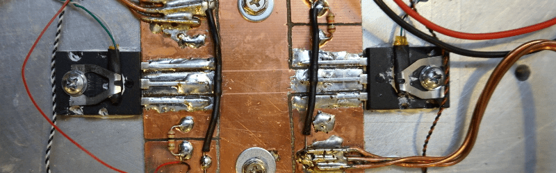
Nice soldering there.
Soldering is fairly nice for this style of prototyping….
My only concern is at the high currents, I’d solder-fill the whole copper plane and/or lay some single-core around the pins to allow the minimum resistance around the pin area due to the copper thickness under the MOSFET pins.
Though for some reason I just preference overkill.
It is a common misconception that blobbing solder over a trace makes it able to handle more current. Solder (60/40 leaded stuff) is a full order of magnitude less conductive than copper, so unless your traces are absurdly thin (like the crap that comes from china with its 10um thick copper layer) you would need to add a millimeter thick layer for it to make any difference.
Where are your numbers coming from? And after that, what about your calculations? As far as I can find the difference in conductivity is about a factor of 6. For standard 1oz or 35um copper that gives you a required solder thickness of 0.21mm for a halving of resistance, under the fairly mild assumption that the trace is much longer than it is wide or thick.
Also, it observably does reduce the resistance. That’s why this is a common trick. Go watch Dave’s video on it for example.
Thanks Wren,
To JRFL: There was an article around here somewhere about soldering to tracks to make a difference in it’s impedance (Or did I see it on another site over a year or so ago?).
From http://www.msed.nist.gov/solder/NIST_LeadfreeSolder_v4.pdf
Resistivity of 63/37 solder is 17uR/cm copper is 1.7uR/cm.
The 2oz copper PCB trace is 70um thick, so you would need 0.7mm of solder just to have the same sheet resistance as the copper trace under it. When you consider spreading effects, you can easily need en even thicker layer to halve the resistance.
Like I said, if you start with a 10um thick trace then sure tinning the trace will make a difference, like the cheap smps supplies you see from china. But in any reasonable copper thickness (such as the 70mil used in this design) the effect is negligible unless you start globing on millimeter thick layers.
jfrl: Sorry, I didn’t see that this project was 2oz copper. Still, 1oz copper is very common and generally cheaper, and solder is deposited for free in a wave solder process if you just leave the solder mask off.
Your 0.7mm figure (for 2oz copper!) still doesn’t sound unreasonable for wave solder deposition — and that’s just for a 50% drop in resistance! Even a 10% drop is not “negligible” and saves you valuable board real-estate for your power-heavy traces. The boost in thermal conductivity and thermal mass is also nice to have.
You can typically half the resistance of the track by this. If this does the job: good, do it. But if I really think about current I would add some copper wires along the trace.
Dave’s video ????
I have ordered a lot of boards from china and every one of them without exception has been on full 1/2oz copper just like I specd out.
“That voltage feeds a comparator which generates the gate voltage after looking at the input control voltage.”
come on is this buzzfeed? These are regular opamps, no comparators. That would make the whole circuit oscillate. It’s a very regular voltage dependent current source.
Opinion dump:
Misuse of components are allowed here (It would be called normal-component-use-a-day dot com otherwise).
Memory dump:
Just read the article and it made sense to me: most datasheets for SMPS/regulator/555/etc using feedback systems describe the feedback as being a comparator As far as I have seen so far.
Personal (Mis-)use case dump:
I have (AB)used 3x comparators two in unity-gain and one as an op-amp in my multimedia laptop custom sub-woofer design in the hope that the lower than op-amp frequency response cap would filter the high frequencies out: Nope, not quite enough so had to use a capacitor/resistor network between the comparator and the sub-woofer amp (with loss of output volume). Still makes a MASSIVE difference in the sound quality.
Make it into an induction heater (:
I tried the feedback loop but had problems with my pullup resistors causing oscillations: perma-dubstep like noise caused by environmental noise pickup (1Mohm Pullups/dividers).
Filtering the inputs were obviously going to affect the stereo speakers, tried it anyway and found I was right…
Final layout was to use two unity gain comparators for stereo separation and to stop the eq affecting the source signal (signal isolation) then I forgot to build the 2-stage feedback “opamp” eq to try and overcome the oscillation issue and increase stability. So I just chucked a resistor and capacitor to filter out the HF.
Will revisiting this in the future for improvements… but until then, Meh! IT WORKS!!! :D
With respect Steve, it is quite common in analogue electronics to use an op-amp and configure it as a comparator.
http://www.analog.com/media/en/technical-documentation/application-notes/AN-849.pdf
That’s a perfect idea for my seed germinator project… I’d stick 4 of them under a big heatsink I have and put my planting pots over it, set the temperature, and let it grow :)
Check out the “quad-386 coffee heater” here:
http://hackaday.com/2016/08/13/hacklet-120-coffee-hacks/
Interesting use for discarded chips.
Power the lights, watering and fans with it too.
I’ve built an electronic load with 14 BU508 bipolars. It’s a little more bulky with its 1m long heatsink…
“However, it does mean you have to carefully select the op amps to have very low input offset voltage as even 1 mV is more than a 1% error at this level.”
You don’t even really have to use an op-amp. The required frequency response is very low – you basically are just compensating for the FET’s temperature coefficient. Fun fact – if you would just set a fixed voltage on the FET to put it in the linear region and just let it go with no feedback, the current would slowly run off to infinity, because the FET’s on-resistance drops with temperature.
So there’s no reason you can’t just use a microcontroller with a PWM output (the FET’s input resistance is huge, so you can filter the heck out of it), read back the sense voltage with an ADC and control the thing closed-loop. Then you can calibrate any errors out in software. I’ve ended up with better than 1% accuracy on a current-controlled heater this way.
Maybe this is good for application that doesn’t require good transcient response. But with a slow response like that, what would happen if you put, let’s say, a high current capable battery on the electronic load ?
Scenario :
– You start off your electronic load, set it to a 10A target
– Feedback control eventually set gate voltage to maximum, let’s say 15V. Enough for RdsON to be minimum, eventually allowing a shit-ton of current because nothing is connected to the electronic load input.
– Plug in your battery pack, thinking it will only consume 10A. Because hey, there’s a feedback control afterall !
– Gate voltage was maxed out, total resistance path (Rbat + RdsON + Rcopper + etc) is so low, that current peaks at let’s say 400A. The microcontroller PWM feedback thing is too slow to react and mosfet is destroyed by too much current.
Oh, definitely, transient responses become an issue- but not quite with the example you’ve got. Obviously you put a few safety catches to look for unconnected loads, and you hard-code in maximum gate voltages, etc. You know what the FET’s response roughly looks like, after all, and if you program it as a 5 ohm resistor and you get no current, then as a 2 ohm resistor and you get no current, you’re not going to get 10 amps at 1 ohm. That’s the benefit of having smarts on the thing.
The first few times I did this, though, I absolutely did have cases where it pegged the current limit because of dumb issues like that, though.
I mean, you’d get the exact same problem if you weren’t careful with the frequency response of the op-amp circuit as well. Connecting something live is always a bit dangerous.
It does not need to be “connecting something live”. Think of a PWM output.
That is even a problem with commercial electronic loads. Put some 12 or 24V PWM output with moderate rise time (30µs) and something like 100Hz on it and you get inrush peaks of 20-30A, probably just limited by the output stage (DUT). I have the suspicion, that they do the stuff also mostly in software.
> the current would slowly run off to infinity
Can you tip us off about where you get your power supplies, Pat? I could find uses for a few of those…
LTSpice has a nice infinite current capable power supply. :)
The FETs on resistance increases with temperature. What often decreases is the threshold voltage. And for a low shunt you have to amplify the sense voltage with a good low-offset amplifier. Of course you can try to compensate anything in software, if your components (offset) are stable enough over time.Otherwise you would have to recalibrate very often :-(
Why not using an amplifier for the current shunt? I use INA214 with a gain of 200 for such purpose. http://kaktuscircuits.blogspot.cz/2014/07/mightywatt-revison-2-now-50-mightier.html
Anyways, nice setup with the huge heatsink! With a SOA of 575 Watts per transistor, there is certainly a possibility to handle big power peaks.
You must be very careful building and using something such as this. Always insulate any exposed contacts. Use lot’s of rubber. You wouldn’t want to blow your load!
It looks like a beefed up reload pro. Maybe the software is better there…
You may also be interested in the latest revision of Jasper’s Electronic Load. It is open source, Arduino compatible and super fast. Current settles in 20us. That’s quick enough to simulated 550us 2A current pulses from GSM modules.
https://www.tindie.com/products/jaspersikken/jaspers-electronic-load-r3/