There are many, many ways to get a PCB design onto a board for etching. Even with practice however, the quality of the result varies with the process and equipment used. With QFN parts becoming the norm, the days of etch-resist transfers and a permanent marker are all but gone. Luckily, new and improved methods of Gerber transfer have be devised in recent years thanks to hackers across the world.
One such hacker, [Henner] is working on a project called LDGraphy in an attempt to bring high-resolution etching to the masses. LDGraphy is a laser lithography device that makes use of a laser and a Beaglebone green to etch the layout onto the board. The best part is that the entire BOM is claimed to cost under a $100 which makes it affordable to people on a budget.
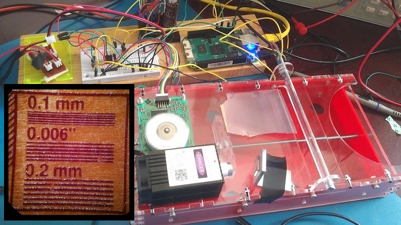
The system is designed around a 500 mW laser and a polygon mirror scanner meant for a laser printer. The board with photoresist is linearly actuated in the X-axis using a stepper motor and the laser beam which is bounced off the rotating hexagonal mirror is responsible for the Y-axis. The time critical code for the Programmable Realtime Unit (PRU) of the AM335X processor is written in assembly for the fast laser switching. The enclosure is, naturally, a laser cut acrylic case and is made at [Henner]’s local hackerspace.
[Henner] has been hard at work calibrating his design and compensating for the inaccuracies of the components used. In the demo video below he presents a working version with a resolution of 6 mils which is wonderful considering the cost of the machine. He also shares his code on GitHub if you want to help out and you can track his updates on Google+.
This is not the first time we’ve seen a DIY laser PCB exposer, of course, but it is one of the best documented. And if you’re looking for other ways to get your clothes stained, how about vacuum exposure or some etching technique tutorials?


Maybe someone can clear this up for me – I’ve seen people build custom agitation rigs for the ferric chloride process – would an ultrasonic cleaner purposed the job work for etching, or would I be just vaporizing toxic chemicals into the air? (It’s also a given that the container would have to be resistant to the dissolving effects of the FC.) It would be a very affordable option if it worked.
What would be the benefit of the ultrasonic agitation? From my experience you want to acheive two goals with agitation: Make shure that your etchant stays well mixed, basically to bring fresh acid molecules to the copper you want to remove, and move away the solved copper. If you have a heater element, you would want to spread that heat evenly over the etchant and board as well. The second is oxygenation. At least the way i understand it, oxygen helps the acid perform better, thats why there are foam-etching and spray-etching machines used with ferric chloride. I only used sodium persulfate for years now, because it is less messy and the resulting quality is better IMHO. I have a heater inside my tank because sodium persulfate needs over 40°C to work properly, and an air bubbler to keep the acid agitated.
Ultrasound is what they use to completely remove microbubbles in the more advanced lithographic systems. It probably will improve etching in the same regard.
I haven’t tried it but here is my thought.
The gentle agitation caused by the bubbler is just to ensure that fresh etching solution is constantly in contact with the copper.
An ultrasonic cleaner uses sound to help clean surfaces. That problem with that is that the resist used to mask off the tracks from the etchant would be removed from the copper exposing all of the copper to the etchant. Vaporization of the etchant would also be a concern.
Neither of these things happen. It doesn’t do much at all.
Perhaps if PCB was placed above the surface of the etchant, and everything kept closed and sealed, then atomized droplets of very well oxygenated etchant would be deposited on all surfaces, including exposed copper of the board to be etched, which should be a good thing, something like a spray-etching
No. I tried it. Didn’t work. I was using a plastic tray of etchant in an ultrasonic cleaner full of water, so maybe that didn’t help. The end result was no effect though.
Holy Moley that is some impressive work. Those are incredible results for something accessible with what amounts to off-the-shelf components nowadays!
Nice, but if you’re trying to be accurate, pay attention to detail. That leadscrew is bent as a banana, and would take only minutes to straighten!
This is actually intentional to test that the drive design is working well when thrown hardware-store quality threaded rods at it. The design allows for two axes of freedom and only drives in one direction – that is best tested with a somewhat wobbly leadscrew.
Most design choices are done to be robust and still create accurate results even with hobby-level precision.
Is there any specific reason why you need a beaglebone green to do this? That board alone costs 50$. I would have thought that a cheaper 32 bit microcontroller, maybe some controller evalboard, would work just as well for the task at hand and only cost half the price of a beaglebone or less. Or if you want to go all powerful with the controller, take something like the STM32F746G-DISCO that offers Cortex M7, USB, ethernet, SD card, 4.3″ graphic touch display and more in one neat package for about the price of a beaglebone.
Reason could be to have a nice web frontend for it, along with gerber files crunching, and other nice features. The actual hard real-time job of controlling the laser is done by the PRU unit on the BBG. This PRU is basically a 32 bit dual core micro, but the main processor of the BBG can run a whole embedded system.
Okay, if you want to feed gerber to the machine, that might make sense. But if you already have a powerful PC that is running your CAE (layout) tools, why not just use that PC power to generate gcode (or what ever machine instruction set you prefer) and only feed the instruction to the motion controller? Would make more sense to me to use the available power as much as possible, and only run the time critical part on the controller.
I doubt that you would have the complete toolchain to create the layout and gerbers on the beaglebone anyway, even if it is probably technically possible, performance would hold you back too much to be productive.
First simple reason: I already had a BeagleBone lying around and had interfaced hardware with it in a previous project (BeagleG), but I had no free Cortex M4 lying around.
You are right, that _only_ doing the realtime critical part, you can use a microcontroller. But there is more to it of course, and I wanted a network appliance that works as PCB exposure device, possibly provides a web-server and also can take a USB stick with Gerbers if needed. In that case, using a $39 BeagleBone Green is all around cheaper and more comfortable to program than if you consider a $35 Raspberry Pi + STM32 + more complicated set-up.
Vat da faak! That is awesome! Really wanted to try this a while back, glad to see someone has eventually. I once added a UV laser diode to my cutter/engraver, but it took forever to expose a board – this is so much faster with the spinning mirror.
I wonder – with a powerful enough laser, would it be possible to essentially hack a laser printer to expose a board in this fashion? Replace the laser diode in the scanner, remove the fusing rollers, but keep everything else the same. Could a high enough power be used to expose the board at “full speed” as it passes through the printer? I’m guessing probably not – you’d need something like a 20W laser to make it work!
That’s a good call — the OP here is essentially building a special-purpose / limited-purpose laser printer, minus most of the fiddly bits — fuser, toner sprayer, etc. You could imagine going the other way: starting with a straight-path laser printer, and hacking away everything that you don’t need.
If you do this, make sure that you get a 1200 DPI machine. 600 DPI ends up being a limiting factor in toner transfer methods.
I happened to re-read the previous article on the laser scanner, and I notice he said that the existing optics were unsuitable, both because of the antireflection coating, but more importantly the different focal point due to the vastly different wavelength. Guess I should’ve realised that first ;-)
Although he seems to be limited by the laser resolution at the moment, I suspect he’d have better results using presensitised board, rather than using dry-film resist which tends to be thicker.
I have not tried the presensitized board with the positive resist yet.
In general, I’d like that, because it simplifies the preparation, as no dry-film lamination is needed. The downside is, that these photoresists are a lot less sensitive, so need a lot more light than dry-film (4x or so ?). I just got an order of these boards, so I might try this over the weekend.
(As a side-note: it seems to be very hard to get presensitized boards at a good price in the US. When I was living in Europe, I usually used the excellent Bungard boards for reasonable prices.)
As for resolution: Yes, the coating on these boards could result in better resolution. Yet right now I think the limits are still mandated by the machine not the resist. Most notably the cheap laser lens there only focuses to an oval dot of 0.08mm/0.1mm. So the 5-6mil resolution I only get due to image pre-processing that takes that into account. Having said that, 6mil is the resolution offered by OshPark, so it is pretty up there.
This is the current resolution I get:
https://plus.google.com/u/0/+HennerZeller/posts/a8taHWeL5CC
Very good results considering your not using an F-Theta lens system to get a flat field on your board! Nice work! I believe it would be very difficult to get much better without some expensive optics upgrades, and a much better mechanical platform.
Very nice and yes challenging the limits of FCL process with regards to timing and temperature with the thin traces. Overall I would love to see this mature to the point of doing 160x100mm boards. Take my money :)
Alright, so this is ready for you :)
The LDGraphy you see in the video is already taking 160x100m boards; the sled is 162x102mm (The sample that I exposed in the video was 100x70mm, so you see that width fits, but the sled is 90mm longer).
Having said that, this is customizable – the PostScript file that generates the cut-pattern has parameters so that you can create larger boards (but: exposure time) or smaller.
Here you see the cut pattern and the size of the sled:
https://github.com/hzeller/ldgraphy/tree/master/hardware#cut-pattern
How about double sided? =)
Stay tuned :)
Beautiful device, must have been very fun to create
but it only solve the picture transfer problem, which is the easiest one in pcb manufacturing.
I have been waiting for years for someone to came with a good idea for plated vias (please no rivets).
Since i can now have my pcbs made online for 5$, all this is less mandatory, i can spend more time on the design than on the making.