For those of us whose introduction to PCB making came decades ago and who share fond memories of permanent markers and crêpe paper sticky tape, the array of techniques available to PCB artists of today seem nothing short of magical. Toner transfer and peroxide etchant mixtures might seem run-of-the-mill to many readers, but even they are streets ahead of their predecessors from times past.
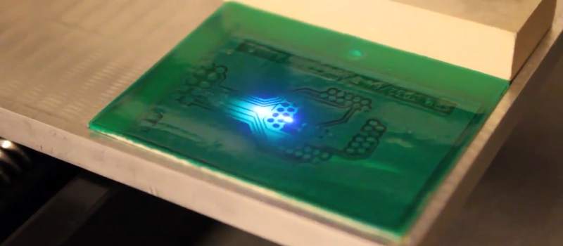
Photographic exposure of etch-resist coating has traditionally been performed with a UV lamp through a sheet of acetate film, but there is no reason why that should be the only way it can be performed. There have been plenty of projects using lasers or LEDs to draw a PCB design onto the coating as a raster, and a rather nice example from [Terje Io] using a Blu-Ray laser diode is the subject of the video below the break.
The diode is mounted on a gantry with a THK KR33 linear actuator that he tells us was unsuitable for his CNC mill due to backlash. This gives a claimed 1200 dpi resolution, over a 100 mm x 160 mm exposure area. Software is provided in a GitHub repository, taking a PNG image exported through a PDF printer. And since it’s got a UV laser, it can be used in a second pass to process UV-responsive soldermask film. ([Terje] cheats and uses a separate CNC mill to drill out the holes.) The result looks great.
Laser PCB exposers have featured here before, for example this BeagleBone-powered example, this one made from scrap CD drives, or this one that repurposes a laser printer’s spinning mirror unit. We’re sure this one will not be the last we bring to you.


How different is G-code from gerber photoplot format? Maybe this could prototype boards with this then send the same gerbers to the board house when your prototypes work.
It’s pretty different. In gerbers, you use predefined shapes and move them across the x-y plane to draw all the features you would like to have in copper on the board. In the g-code you move around a tool that removes material so you are left with the structure you want in copper. So you can’t just do a “simple” 1:1 translation. You have to first draw all the copper defined in the gerber file, and then you can trace the edge of that image to make a toolpath for your g-code commands.
If you had a very smart control system with a high resolution micro mirror array in the light path, you could probably recreate the gerber aperture shapes and move them around directly to do the exposure without translating gerber to g-code, but since you can basically define any aperture shape in the extended gerber format you would need some really smart software and possibly still be limited in the apertures you can recreate. And on top of that, you still need a way to control the amount of light (exposure) that hits your board in order to get a clean and consistent amount of exposure over the complete layout. So, converting the gerber into a g-code that can be rasterized onto a board surface is way easyer and better imho.
it is incredibly different. gerber describes polygons to be exposed with light, while g-code describe movements of a tool. source: I have developed parsers and generators for both ( https://github.com/nraynaud/webgcode/tree/gh-pages/webapp/cnc/import, https://github.com/fritzing/fritzing-app/pull/3083, https://github.com/nraynaud/webgcode/tree/gh-pages/webapp/cnc/gcode, https://github.com/nraynaud/webgcode/blob/gh-pages/webapp/cnc/cam/cam.js#L275 )
I am using KiCad for my designs and I do not involve gerbers for exposing the pcbs. KiCad has an option for “plotting” to pdf-format files, and does so by outputting some kind of vector format – I assume so since when I zoom a file to 6400% there is no visible pixellation. I then “print” the PDF via the PDFCreator printer driver to a bitmap file (png) that I use for rendering. PDFCreator is great for this as it allows me to specify the exact resolution I want. For drilling I use excellon-format files converted to gcode for Mach 3.
I have made a couple of boards that I have prototyped first by using the exposer, after verifying the design I just “plot” to gerber-formatted files instead of pdf. I then a do visual inspection of the resulting gerber-files before I send them off to the board house.
G-code is typically generating the negative of the finished item while Gerber is generating the positive. Both of them do generate vector paths, but Gerbers also have the notion of special shapes which G-code doesn’t. For example, a Gerber can print a triangle or a half-circle or any other random shape in a single step, much like a character in a font; there’s no match in g-code.
Gerber was originated for use in X-Y photoplotters, which used aperture wheels that had pre-defined shapes, and could either flash a lamp to create a spot that matched the shape, or be on continuously to use an aperture to draw a line.
G-code was to drive an X-Y(-Z) movement and any tool size/shape is not part of the coding. It does have special options for spindle speed and the control of other items, such as coolant.
Where many formats overlap is when they can create a bitmap of the finished item. This can be used to create a positive or negative film and then the correct view can be generated for etching the final board.
The missing piece is a g-code to bit-map convertor, which is similar to what machining simulators do. I think a conversion from g-code to PDF would be the easiest start along that path.
This is one of the reasons I bought a laser etcher. Of course I wish there was a good SVG plugin for Eagle that exported traces and through hole. Converting from an image output, even at 1200DPI ends up with issues. I know there’s a G-Code plugin, but it will only do through hole for drill output.
Have you tried pcb2gcode?
No I haven’t tried it, but looks like it would need a little work to get it going for a laser etcher.
I don’t know what format your laser etcher requires, but I’ve found that toner transfer works best if all image processing is done in vector formats. The process I’m using now (after many less-than-satisfactory attempts to do otherwise) includes exporting as EPS (through the CAM processor), followed by importing into Inkscape for processing, then saving as SVG or PDF for future use, then printing from the generated PDF file. Printing from raster images tended to turn thin (0.2 mm) traces into squiggly lines and make trace clearance irreproducible, even before the toner transfer itself.
Mine takes in GCODE format. I can convert SVGs to GCODE – but sometimes that’s not the best.
It makes no sense to draw a vector-drawing in pixel if you use a mechanism, that is capable to draw it in vectors.
You get a nearly infinite resolution and higher speed.
https://www.mikrocontroller.net/topic/391759
Translation:
https://translate.google.de/translate?sl=de&tl=en&js=y&prev=_t&hl=de&ie=UTF-8&u=https%3A%2F%2Fwww.mikrocontroller.net%2Ftopic%2F391759&edit-text=&act=url
The resolution will be limited by the photosensitive material, the Dupont Riston film I have used so far is limited to 75um (3 mil) in a production environment and 50um in a lab environment. At 1200 DPI the exposers resolution is ~20um (mechanical), what the exact resolution at the exposed film is I do not know but it is good enough to faithfully reproduce the edge cut lines which are aproxximately 0.12mm (6 pixels) thick. So, for me it made sense to rasterise since it is far simpler to program, the MSP430G2553 I used is cheap and does the job just fine even as it has only 512 bytes of RAM available.
That looks very professional.
What is the cost of the build?
Are there any inexpensive kits from China which I can order to use for this? ( I don’t mind having a smaller area inside the rails, I also don’t need drilling)
The bad THK KR33 linear actuator was 220 USD from eBay, linear bearings was USD 60 for two (I have one spare). So I guess around USD 350 plus quite a few hours work to get it right. I am thinking of making the mechanical design simpler and cheaper by replacing the linear actuator with a linear bearing and drive the bed with a belt. However, the biggest stumbling block for most hobbyists may be that the parts has to be machined out of aluminium.
“For those of us whose introduction to PCB making came decades ago and who share fond memories of permanent markers and crêpe paper sticky tape, the array of techniques available to PCB artists of today seem nothing short of magical.”
Puppets, that was pre-made pads and other pieces transferred to the film with an x-ecto knife.
I wonder why someone hasn’t hacked together a laser and high speed motor (drill/dremel/whatever…I love me some 3 phase quadcopter motors BTW) into one moving head unit so both devices are opposite each other. A servo or even a solenoid could rotate the head 180 degrees when it’s time to change functions. Another example could be a vacuum pick and place device and a solder paste dispenser. Since they would be 180 degrees apart, they wouldn’t interfere with any axis.
Bah, hardware (not electronics…) is easy. It’s the damn software that’s the problem.
That rotating head idea actually reminds me of revolver pick and place machines that load up a few nozzles with components in the pick-up area and then move to the board to place them. Saves quite a bit of time if you can reduce the back and fourth movements between the board and pick-up area.
This has spurred me on to get back to my direct exposure project :)
https://www.youtube.com/watch?v=PEWq3v3ilcc&feature=youtu.be
I am trying to make as much as possible either 3D printable or laser cuttable.
I am using a Tiva Launchpad at the moment but will build a custom board once things are going the way I want them to.
Terjeio, what laser are you using? Do you do any active focusing? Will you be releasing more information on your laser setup since I would love to try to integrate some of your work and possibly replace the PS3 module I am using since it is a bit cumbersome, although it does have the advantage of being able to focus, and also has a red laser for alighment testing etc…
The laser is a Sony SLD3235VF (100mW/405nm IIRC), any BluRay writer diode should be ok. I keep focus constant as that is giving me consistent results. My design has an option of controlling the focus (Z-axis) as I mounted the diode on a “sledge” from an old Sony 3 1/2″ floppy drive – but I have never used that, IMO not needed. The diode is mounted in a brass mount with an adjustable lens (search for “brass laser diode host” on eBay) and the distance from the laser host to the PCB to be exposed is 70 mm.
Initially I bough a laser driver off eBay, but it was way too slow so I made my own – you will find details of that in the KiCad schematic available on GitHub.
There is one important detail to be aware of, I am using a GT2 belt and a 17 teeth pulleys in combination with 8 microsteps for a 200 steps/rev motor to get 1200 DPI mechanical resolution on the X-axis (actually ~1196 DPI). This simplifies rendering as one pixel equals one microstep. The Y axis could also be belt driven but I opted for the linear actuator as I had that lying around.
The mecanical design is available for download at 43oh.com, the files are in Vectric format. A link can be found on GitHub in the PCBLaserFirmvare project. If I get around to make another exposer I will simplify the design to two belt driven axes and publish the mechanical design on GitHub.
Or should we start a project on Hackaday.io?
Hmm. OK. You have now got me thinking… I think I will try using a discrete laser diode (I have a few 805T diodes and housings) since it looks like you got fantastic results with your solution.
Using Gt with 16 tooth pulleys. Currently 8 micro-steps too but easily changeable. The Tiva firmware builds a line buffer for each source file ‘step’ distance in each direction so both the source image DPI and controller steps per mm can be changed easily (since I don’t have a good feel yet what the best settings will be)
I think I am going to throw a diode driver together and print a new carriage that can take the fixed laser diode. It will be a lot quicker to get running than the PS3 carriage.
Do you know if there is a way to message each other to swap e-mail addresses?
I am certainly open to putting everything into a Hackaday.io project. Would like to see myself actually print something first though :) Now a big fan of vaporware and I tend to start a lot of projects that never see the light of day.
Your work has certainly kicked me on :)
I have added a project to hackaday.io, https://hackaday.io/project/26216-pcb-exposer
We can use team messaging for communicating, I have to learn how to use it though.
Wonder if a direct blue diode would work? PL450 has a tiny focal spot.
Possibly, but at 450 nm it is at the edge of the sensitvity range for Dupont Riston film that I am currently using. The datasheet states that it responds best to UV light in the 350-380 nm range, a BluRay diode emits at 405 nm so is pretty close. There is some sensitivity from 300 to 450 nm as per the datasheet so you may give it a try. Other photosensitive material may have different properties, however I would guess most are sensitive in the UV-range.