We are now in a golden age of printed circuit boards. It wasn’t too long ago that making your own circuit boards either involved a lot of money, or slightly less money and using some proprietary garbage PCB layout tool. Now, every board house speaks Gerber, and you can get a ten-pack of PCBs from China for five bucks. This incredible cost reduction means people are making art with printed circuit boards. We’ve seen portraits, landscapes, and memes. This is truly the beginning of a new artistic medium rendered in fiberglass and soldermask.
Check out this blinky bit of art nouveau. There is a facebook group for PCB paintings, and some of the Badgelife crew are relying on woodcut and linoleum engraving techniques to create works of art in copper and fiberglass.
For this week’s Hack Chat, we’re going to be talking all about PCB artwork. Our guest for this week’s Hack Chat will be [Andrew Sowa], an electrical engineer, a vocal advocate of KiCad, and the guy who made more of me money. The Benchoff Nickel was created by simply taking some of the fantastic illustrations from Hackaday’s own [Joe Kim] and applying KiCad’s Bitmap2Component tool. Since the creation of the nickel, [Andrew] has been working on extending his technique to cross-hatching, backlighting, and halftones.
In this Hack Chat, we’re going to be talking all about PCB artwork, including the very beginnings of PCB art where engineers hid a few easter eggs in the PCBs of Xboxen and other consumer electronics. Topics covered will be bitmap to SVG conversion (in Inkscape and Illustrator), KiCad footprint creation, and the more technical side of things with the limitations of PCB fabrication and the slightly different shades of beige FR4 comes in.
Our Hack Chats are live community events on the Hackaday.io Hack Chat group messaging. This week is just like any other, and we’ll be gathering ’round our video terminals at noon, Pacific, on Friday, April 20th. How can there be time zones when the Earth has four days simultaneously for each rotation? You erroneously measure time from one corner. Here’s a clock counting down the time until the Hack Chat starts.
Click that speech bubble to the right, and you’ll be taken directly to the Hack Chat group on Hackaday.io.
You don’t have to wait until Friday; join whenever you want and you can see what the community is talking about.

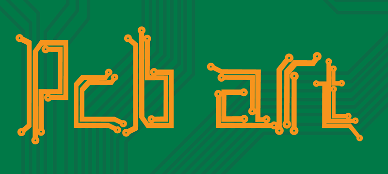



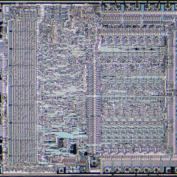



a bit of promotion as it’s close related to topic
https://hackaday.io/project/28474-pic-o-matic
A while back, I did a run of Celtic-inspired PCB coasters – http://www.imajeenyus.com/electronics/20150227_pcb_coasters/index.shtml
2.4mm FR4, black soldermask, gold-plated tracks.
Where’s the Arduino? Blinkenlights?
B^)
(cool work actually!)
should we put questions in as comments on the event page? https://hackaday.io/event/112119-pcb-artwork-and-photo-conversions
We could…
but I forgot my .io password,
(actually I have it somewhere, and if I request another/reset I’ll probably misplace that one too!)
B^)
…waiting for my MooltiPass Mini to arrive…
This topic interests me a lot, thanks for bringing it up. It’s also a bit of self-promotion, I’m creating a lot of what I call PCB Drawings, basically non-functional circuit boards as art objects. You can see some at http://tibichelcea.net/pcb-drawings/. They are all pretty small (4×4″), though lately I’ve started to make some larger ones (22×22″).
Your artwork is wonderful. What software/process are you using to convert artwork to gerber?
Hi TJ, thank you! I’m not converting any previously designed artwork into a circuit board model/gerber. I design everything in Eagle from scratch, using its UI (for the most part). For some designs, I write short C# programs to output parts of the design (i.e. some XML that can be copied into the .brd file). Once I’m satisfied with the design, I export it into Gerber using Eagle’s CAM processor. Hope this helps.
I just throw a Inkscape plugin in here:
https://github.com/badgeek/svg2shenzhen-next
Written by a friend of friends.
sure hope you’ve got saar in the chat. Boldport FTW !!
Another inkscape plugin which exports footprints which can be imported into gEDA PCB, pcb-rnd and KiCad
https://github.com/erichVK5/inkscape2pcb
Also, the cross platform FOSS 2D CAD package FidoCadJ can export cubic splines, beziers and PCB artwork in gEDA PCB format, as used in the following (obligatory) arduino powered flying spaghetti monster
https://hackaday.io/project/19904-noo-dleus-ex-machina-freeform-pcb-design-proto
https://cdn.hackaday.io/images/original/3967891489150549937.gif
The process of importing vector-based formats to PCB is still FAR more complicated and error prone than it should be. DXF or SVG to PCB is super annoying, although there are scripts out there. This should be supported by KiCAD and others out of the box so it’s easy to use CAD to make PCB copper-based components. I’ve managed to do all this, but I actually gave up trying to import vectors, and instead wrote a Python script to write/modify a design into my KiCAD board file from scratch (i.e. I specified the shape algorithmically/mathematically in the Python script). This needs to be improved dramatically.
+1