The availability of low-cost, insanely high-quality PCBs has really changed how we do electronics. Here at Hackaday we see people ditching home fabrication with increasing frequency, and going to small-run fab for their prototypes and projects. Today you can get a look at the types of factory processes that make that possible. [Scotty Allen] just published a (sponsored) tour of a PCB fab house that shows off the incredible machine tools and chemical baths that are never pondered by the world’s electronics consumers. If you have an appreciation PCBs, it’s a joy to follow a design through the process so take your coffee break and let this video roll.
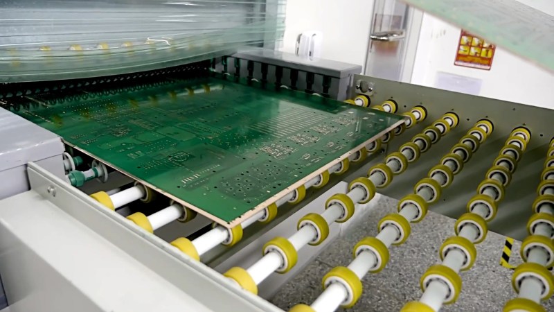
Several parts of this will be very familiar. The photo-resist and etching process for 2-layer boards is more or less the same as it would be in your own workshop. Of course the panels are much larger than you’d ever try at home, and they’re not using a food storage container and homemade etchant. In fact the processes are by and large automated which makes sense considering the volume a factory like this is churning through. Even moving stacks of boards around the factory is show with automated trolleys.
What we find most interesting about this tour is the multi-layer board process, the drilling machines, and the solder mask application. For boards that use more than two layers, the designs are built from the inside out, adding substrate and copper foil layers as they go. It’s neat to watch but we’re still left wondering how the inner layers are aligned with the outer. If you have insight on this please sound off in the comments below.
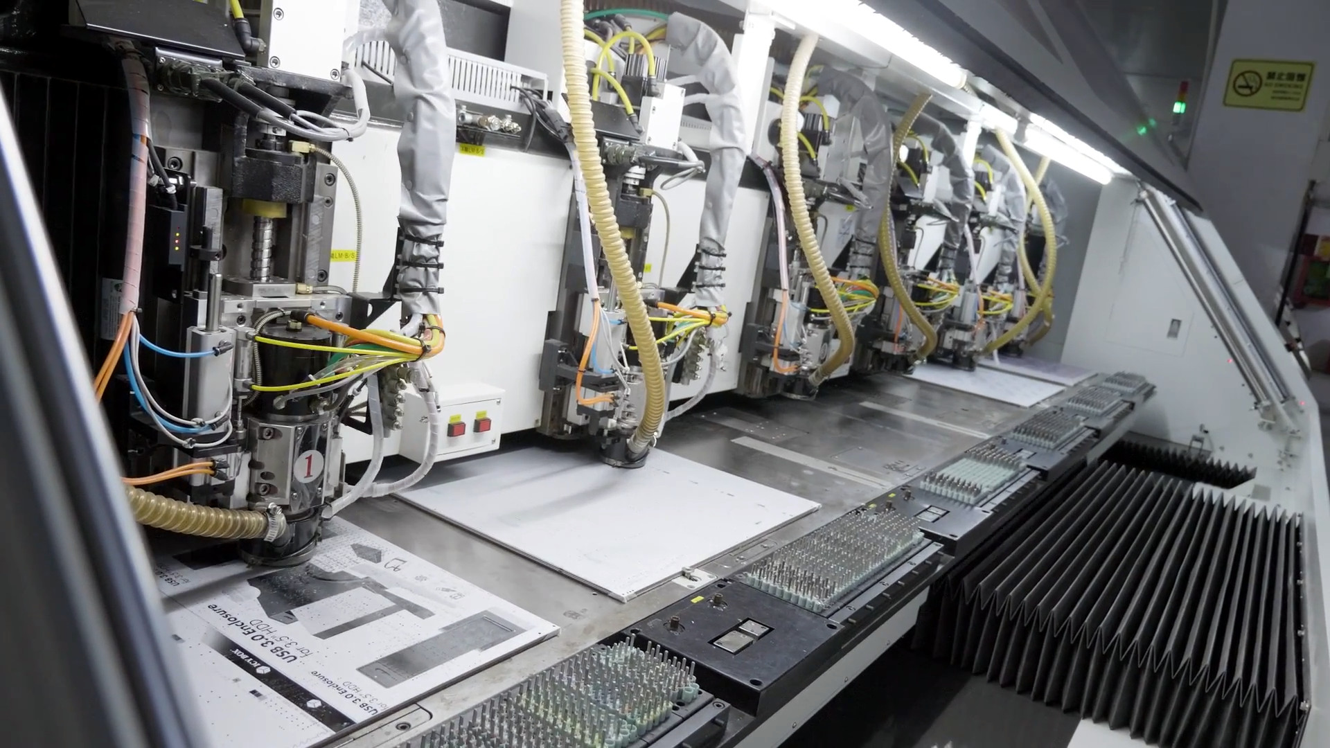
The drilling process isn’t so much a surprise as it is a marvel to see huge machines with six drill heads working on multiple boards at one time. It sure beats a Dremel drill press. The solder mask process is one that we don’t often see shown off. The ink for the mask is applied to the entire board and baked just to make it tacky. A photo process is then utilized which works much in the same way photoresist works for copper etching. Transparent film with patterns printed on it cures the solder mask that should stay, while the rest is washed away in the next step.
Boards continue through the process to get silk screen, surface treatment, and routing to separate individual boards from panels. Electrical testing is performed and the candy making PCB fab process is complete. From start to finish, seeing the consistency and speed of each step is very satisfying.
Looking to do a big run of boards? You may find [Brian Benchoff’s] panelization guide of interest.


“…wondering how the inner layers are aligned with the outer. If you have insight on this please sound off in the comments below.”
Just a guess, but I would think it would be something similar to the process used to ensure registration in four-color printing.
Dunno how they plate through holes these days…
But I visited a small PCB house in roanoke, VA a couple-three decades ago, and for 2 sided boards I saw the process on, they used a weak solution of palladium chloride (about 1%) as a dip which deposited in the holes, wiped the top and bottom of the board, then dipped it electroless copper plate to get the initial plate. Then they electroplated on thicker copper all over the board and in the holes.
Following that, the holes were drilled with their robot. Then the photosensitive film was placed and exposed. They did this “backwards” in that after developing, the holes and traces were exposed, which then had solder (or later, gold) electroplated on them. This solder (weird chemistry no doubt) or gold served as the resist for the actual final etching.
So alignment of the artwork was done *after the holes*, making it easy. This shop was at the time (~80s) struggling to produce multilayer boards competitively at all.
Believe me, at that time almost no home gamers could do boards at home, and none of us could afford the multi k$ setup, or the (in once case I know of) >$7k for layout and taping (yup) of a 100 in sq 4 layer board.
Those presensitized PCBs and inkjet or laser printers were a huge deal to us, and home game boards started to appear “at all” – radio am handbooks at the time had you dremel out islands and do point to point on fr4, or a little later you could get stickers with copper on top and adhesive on the bottom. A “Real pro” home gamer had wire wrap, the rest just point to point soldering before that point in time.
Toner transfer came as a cheap low quality alternative after the photosensitive board. For awhile, you could buy spray on photo resist, but unless you made a spin coater (exotic hack — drill in a cardboard box in the darkroom) it wasn’t real usable. Thickness variations mattered as it was linear – more light, faster wash-off, thicker film, slower – too many variables made it real hard).
Probably all different today…what with actual computers instead of taping up at 4::1 scale and having it shot down in a large format camera at the sign shop (no one else had cameras that big).
Edit, sorry, holes were all drilled FIRST and used as registration for all following steps. I have no doubt there are far better ways now.
At any rate PdCl was used to catylze the electroless copper to plate just enough in the holes to allow electroplating later.
AP Circuits in Canada more recently explained to me (only a decade and a half back) that one reason for the design rules was still alignment of holes with pads. The drill might walk a little or the art or resist shift a bit…those fudge factors seem to be getting smaller all the time.
As pointed out in an earlier article, what used to be almost insurmountable is now cheap and fast, and you can even chose the colors!
So we can have our nasally fitted fire the way we want (HHGTTG).
I would definitely bet that they still use a palladium chloride bath then a stannous chloride sensitizer reduction to precipitate nanoparticle palladium then electroless copper via reducing agent of sodium borohydride, sodium hypophosphite or hydrazine hydrate to plate copper in the holes. It’s really not very costly as the palladium solution is 0.1 molar or less. You could definitely do this at home if you can get ahold of some sodium hypophosphite or even synthesize some hydrazine hydrate yourself.
It isn’t necessary to have a spin coater for the liquid photoresist. Nearly 40 years ago, we used a square of toilet paper to drag a small puddle of photoresist to an even coating over the whole board – just drag alternately in X and Y, then X again, holding the paper at a low angle. Prior cleaning of the copper required greater fastidiousness. A drop of water was not allowed to pearl on the surface, or the photoresist wouldn’t stick adequately. Taping top & bottom negatives to a long thin PCB offcut maintained registration for two sided boards, and a suntan lamp provided UV. It was admittedly tedious to solder bits of wire into vias on our home-brew boards, so through connections were kept to component leads where possible.
The give-away price of the 10 boards I had back from China a week ago makes me glad we no longer have to do it the hard way, though.
Inner layer fiducial location marks can be found by using X-rays, and then registration holes are punched. Later in the process pegs on the various machines fit in the registration holes to line up the photo masks. The pegs also hold the panel in the right place for the drilling machine. Understanding a bit about how the various errors from the x-ray, and the hole punching add up in the process goes a long way to understanding some of the design rules like ‘minimum annular ring’ and ‘minimum anti-pad’ on the inner layers.
The Eurocircuits video shows lots of details… (I have no affiliation with them, the video is excellent and goes into nice detail on the process.)
https://www.youtube.com/watch?v=sIV0icM_Ujo
ha, you beat me to it, should of refreshed before posting :)
re alignment: Eurocircuits video shows stakes:
https://www.youtube.com/watch?v=T7S40GYESbY
Mental image of a fat kid getting sucked up by a gigantic solder sucker or shop vac and a rude little girl being disposed of down the waste reject chute extra… Tehe
What I wanna know is how they make a Rigid-Flex PCB. Those are really magical, and I have no idea how they make it.
The flex layers are usually only on the outside. So you start by making a normal PCB with rigid cores, mill out the parts where there will be flexible layers only, and then sandwich on top of that the flexible pieces, as you would with normal multilayer production. The trick is to have enough rigid parts in the desing so that the panel can sitll run thru the production lines. So you add quite a bit of support structure around the flex parts that will be cut away once the board is done.
I just received some boards from JLCPCB today! I dont agree with the claim at the end that my order would show up in 3-4 days… Mine was about two weeks. I wo der if it’s because I’m only doing ten copies (using their $2 for 10 copies deal). I suspect they’re filling up a panel with many designs, not just my own, and slipping that into their production line when there’s room.
You know that you can track the execution of your order on their site? It was 2 days for me before submitting and shipping, but I never tried DHL shipping because it’s bloody expensive.
I send a small design on friday afternoon, get done in the weekend and shipping take four days from china to europe. I guess the panels were filling fast this week.
Yes shipping is slower than fab, even by dhl.
Got my JLC pcbs today also 5 days delivered by dhl :)
One method of aligning the inner layers after lamination is using x-rays – I think this is shown in the Eurocircuits video.
Alignment details lacking in the JLC video – as they pre-machine the panel edges maybe they just reference ftom the edges.
I just asked Lily from JLCPCB via WeChat, and she clarified they align the different layers for four layer boards by punching alignment holes on the inner layer, and then find them again after laminating the outer copper layers using x-ray. I’m sad I missed including this in the video. It was a ton of different steps in different rooms in different buildings to juggle though, so not super surprising something fell through the cracks.
Thanks for the update and the interesting video! I have been wondering how this is done for ages
Anyone else get the impression that all the “clean room” stuff was mainly for show? Communal air showers, no beard cover, no gloves in lots of places (and ridiculously ill-fitting ones where they are used).
Very interesting to see the scale of their operation though, I’ve been thinking of buying some boards from them for a while because of the panelisation allowances.
One thing i missed here are the more advanced steps for HDI boards. Like laser drilling for microvias and blind/burried vias. Plugging and covering of vias for via-in-pad or vaccum-tight PCBs and stuff like that. We were visiting the Würth prototype pcb factory in germany a few years ago, and it was very interesting to see these machines live in action. The scale of the operation is quite a bit larger in this chinese factory tho.
I was doing a short internship at Posalux too, one of the companys that make these gigantic PCB drilling machines. I’m still impressed when i see these spindles to theyr tapdance routines… :)
Yeah, I would have liked to see their setup for microvias and blind/buried vias. Unfortunately, while they do do them AFAIK, they don’t do them at this factory – they do them at one of their other locations.