A New Way To Produce PCBs With Your 3D Printer

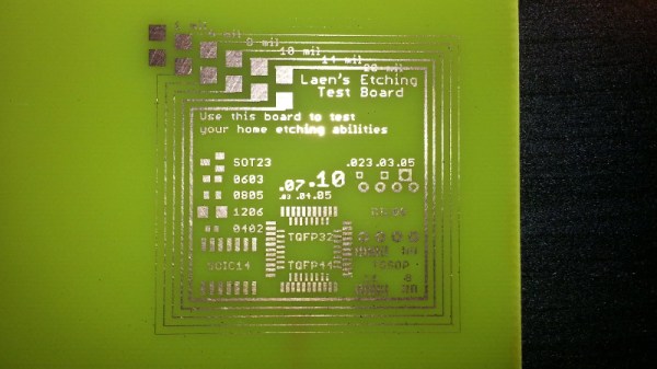
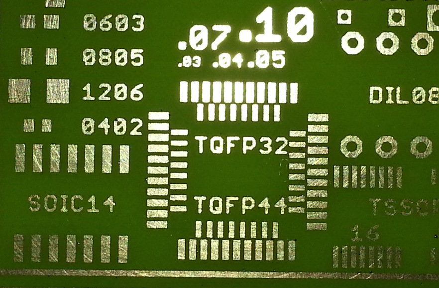
With the low-cost PCB fabrication services available to hackers and makers these days, we’ll admit that making your own boards at home doesn’t hold quite the appeal that it did in the past. But even if getting your boards professionally made is cheaper and easier than it ever has been before, at-home production still can’t be beat when you absolutely must have a usable board before the end of the day.

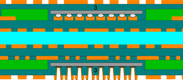
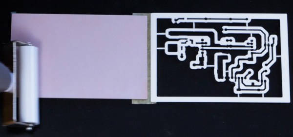
If you find yourself in such a situation, this new method of DIY PCB production detailed by [Adalbert] might be just what you need. This unique approach uses a desktop fused deposition modeling (FDM) 3D printer throughout all of its phases, from creating a stencil based on the exported board design, to warming the UV soldermask to accelerate the curing process. It may not be an ideal choice for densely packed boards with fine-pitch components, but could definitely see it being useful for many prototypes.

Continue reading “A New Way To Produce PCBs With Your 3D Printer”

Get Your PCBs Made At The Mall

As we’ve seen with some recent posts on the subject here at Hackaday, there seems to be a growing schism within the community about the production of PCBs. Part of the community embraces (relatively) cheap professional fabrication, where you send your design off and get a stack of PCBs in the mail a couple weeks later. Others prefer at home methods of creating PCBs, such as using a CNC, laser engraver, or even the traditional toner transfer. These DIY PCBs take some skill and dedication to produce, but the advantage is that you can have the board in hand the same day you design it. But there may be a third option that seems to have slipped through the cracks.

[Virgil] writes in with a very interesting method of producing professional looking prototype PCBs that doesn’t involve weeks of waiting for the results, nor does it require any complicated techniques or specialized equipment. In this method, a UV printer is used to deposit your mask directly onto the copper clad board, which you then etch with whatever solution you like. Don’t have a UV printer you say? No worries, there’s probably somebody at the mall that does.

As [Virgil] explains, the little kiosks at the mall which offer to personalize items for customers generally use a UV printer which allows them to shoot ink on nearly any material. Instead of asking them to put a logo on the back of your phone, you’ll just be asking them to put the vector file of your mask, which you can bring along on a USB flash drive, onto the bare copper board. They may tell you they can’t guarantee the ink will stick to the bare copper, but just tell them you’re willing to take the risk. It’s one of those situations in which your money will be glad to speak on your behalf.

After the UV printer does its thing, the mask might be somewhat fragile. [Virgil] likes to wrap the boards in plastic for the ride home to make sure they don’t get damaged. Then it’s a quick dunk in the etching solution followed by a rinse and some isopropyl alcohol to get the remainder of the UV ink off. The results really do speak for themselves: nice sharp lines with exceptionally little manual work.

We’ve covered some relatively easy ways of quickly producing nice PCBs at home, as long as you don’t mind spending a couple hundred US dollars to get the hardware together. This seems to be the best of both worlds, though it does have the downside of requiring you speak with another human. We’d love to hear from any readers who give this particular method a shot.

Continue reading “Get Your PCBs Made At The Mall”

Scotty Allen’s PCB Fab Tour Is Like Willy Wonka’s For Hardware Geeks

The availability of low-cost, insanely high-quality PCBs has really changed how we do electronics. Here at Hackaday we see people ditching home fabrication with increasing frequency, and going to small-run fab for their prototypes and projects. Today you can get a look at the types of factory processes that make that possible. [Scotty Allen] just published a (sponsored) tour of a PCB fab house that shows off the incredible machine tools and chemical baths that are never pondered by the world’s electronics consumers. If you have an appreciation PCBs, it’s a joy to follow a design through the process so take your coffee break and let this video roll.

Several parts of this will be very familiar. The photo-resist and etching process for 2-layer boards is more or less the same as it would be in your own workshop. Of course the panels are much larger than you’d ever try at home, and they’re not using a food storage container and homemade etchant. In fact the processes are by and large automated which makes sense considering the volume a factory like this is churning through. Even moving stacks of boards around the factory is show with automated trolleys.

Six headed PCB drilling machine (four heads in use here).

What we find most interesting about this tour is the multi-layer board process, the drilling machines, and the solder mask application. For boards that use more than two layers, the designs are built from the inside out, adding substrate and copper foil layers as they go. It’s neat to watch but we’re still left wondering how the inner layers are aligned with the outer. If you have insight on this please sound off in the comments below.

The drilling process isn’t so much a surprise as it is a marvel to see huge machines with six drill heads working on multiple boards at one time. It sure beats a Dremel drill press. The solder mask process is one that we don’t often see shown off. The ink for the mask is applied to the entire board and baked just to make it tacky. A photo process is then utilized which works much in the same way photoresist works for copper etching. Transparent film with patterns printed on it cures the solder mask that should stay, while the rest is washed away in the next step.

Boards continue through the process to get silk screen, surface treatment, and routing to separate individual boards from panels. Electrical testing is performed and the candy making PCB fab process is complete. From start to finish, seeing the consistency and speed of each step is very satisfying.

Looking to do a big run of boards? You may find [Brian Benchoff’s] panelization guide of interest.

Continue reading “Scotty Allen’s PCB Fab Tour Is Like Willy Wonka’s For Hardware Geeks”

The Components Are INSIDE The Circuit Board

Through-hole assembly means bending leads on components and putting the leads through holes in the circuit board, then soldering them in place, and trimming the wires. That took up too much space and assembly time and labor, so the next step was surface mount, in which components are placed on top of the circuit board and then solder paste melts and solders the parts together. This made assembly much faster and cheaper and smaller.

Now we have embedded components, where in order to save even more, the components are embedded inside the circuit board itself. While this is not yet a technology that is available (or probably even desirable) for the Hackaday community, reading about it made my “holy cow!” hairs tingle, so here’s more on a new technology that has recently reached an availability level that more and more companies are finding acceptable, and a bit on some usable design techniques for saving space and components.

Continue reading “The Components Are INSIDE The Circuit Board”

Panelizing Boards The Easy Way

For reasons that will remain undisclosed until some time in the future, I recently had a need to panelize a few PCBs. Panelization is the art of taking PCB designs you already have, whether they’re KiCad board files, Eagle board files, or just Gerbers, and turning them into a single collection of PCBs that can be sent off to a fab house.

Now this is panel racing

If you’re still wondering what this means, take a look at the last board you got from OSH Park, Seeed, Itead, or Dirty PCBs. Around the perimeter of your board, you’ll find some rough spots. These are ‘mouse bites’ and tabs, places where the boards are strung together to form a gigantic rectangular panel sent off to a manufacturer. You can check out this great interview with [Laen] from OSH Park to get an idea of how this works, but the basic process is to take a bunch of Gerbers, add tabs and mouse bites, solve the knapsack problem, and send the completed panel off to a board house.

Panelizing boards is something most of us won’t have to do often. Really, you only want a panel of boards when you’re manufacturing something. For small-scale production and prototypes, bare boards will do just fine. Simply by virtue of the fact that panelizing boards is far less common than throwing some Gerbers at OSH Park or Seeed, there aren’t many (good) tutorials, and even fewer (good) tools to do so. This is how you panelize boards quickly and easily using Open Source tools.

Continue reading “Panelizing Boards The Easy Way”

[CNLohr]’s Glass PCB Fabrication Process

One of [CNLohr]’s bigger claims to fame is his process for making glass PCBs. They’re pretty much identical to regular, fiberglass-based PCBs, but [CNLohr] is building circuits on microscope slides. We’ve seen him build a glass PCB LED clock and a Linux Minecraft Ethernet thing, but until now, [CNLohr]’s process of building these glass PCBs hasn’t been covered in the depth required to duplicate these projects.

This last weekend, [CNLohr] put together a series of videos on how he turns tiny pieces of glass into functional circuits.

At the highest level of understanding, [CNLohr]’s glass PCBs really aren’t any different from traditional homebrew PCBs made on copper clad board. There’s a substrate, and a film of copper that is etched away to produce traces and circuits. The devil is in the details, and there are a lot of details for this build. Let’s dig deeper.

Continue reading “[CNLohr]’s Glass PCB Fabrication Process”

A Low-Cost Mini PCB Printer

The next great advancement in homebrew electronics is an easy way to turn copper clad board into functional circuit boards. This has been done since the 60s with etch resist pens, sheets of etch resist rub-on transfers, the ever-popular photocopy and clothes iron, and now with small CNC mills. It’s still a messy, slow, and expensive process. [johnowhitaker] and [esot.eric] are trying to solve the latter of these problems with a mini PCB printer made out of DVD drives.

Playing around with the guts of a DVD drive is something [john] and [eric] have been doing for a while now, and for good reason. There’s a lot of interesting tech in DVD drives, with motors, steppers, and gears able to make very, very accurate and precise movements. Most PCBs aren’t very big, either, so a laser cutter that can only traverse an area a few inches square isn’t that much of a downside in this case.

With a small diode laser mounted to a CNC gantry constructed out of DVD drives, the process of making a PCB is actually pretty simple. First, a slurry of laser printer toner and alcohol is applied to the board. Next, the laser on this PCB printer lases over the traces and copper fills, melting the toner. The board is removed, the excess toner wiped off, and the unwanted copper is melted away. Simple, even if it is a little messy.

Of course this method cannot do plated traces like your favorite Internet-based board house, but this does have a few advantages over any other traditional homebrew method. It’s cheap, since CD and DVD drive mechanisms are pretty much standardized between manufacturers. It’s also easy to add soldermask printing to this build, given that soldermasks can be cured with light. It’s a very cool build, and one that would find a home in thousands of garages and hackerspaces around the world.

The HackadayPrize2016 is Sponsored by: