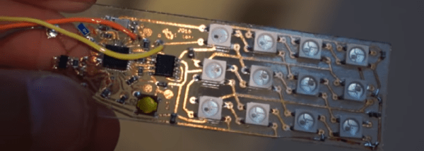
The availability of low-cost, insanely high-quality PCBs has really changed how we do electronics. Here at Hackaday we see people ditching home fabrication with increasing frequency, and going to small-run fab for their prototypes and projects. Today you can get a look at the types of factory processes that make that possible. [Scotty Allen] just published a (sponsored) tour of a PCB fab house that shows off the incredible machine tools and chemical baths that are never pondered by the world’s electronics consumers. If you have an appreciation PCBs, it’s a joy to follow a design through the process so take your coffee break and let this video roll.
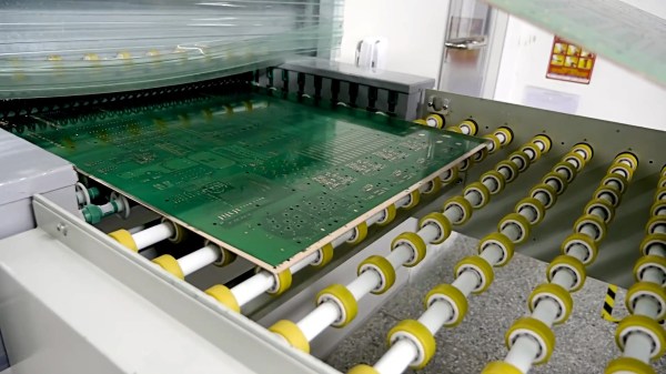
Several parts of this will be very familiar. The photo-resist and etching process for 2-layer boards is more or less the same as it would be in your own workshop. Of course the panels are much larger than you’d ever try at home, and they’re not using a food storage container and homemade etchant. In fact the processes are by and large automated which makes sense considering the volume a factory like this is churning through. Even moving stacks of boards around the factory is show with automated trolleys.
What we find most interesting about this tour is the multi-layer board process, the drilling machines, and the solder mask application. For boards that use more than two layers, the designs are built from the inside out, adding substrate and copper foil layers as they go. It’s neat to watch but we’re still left wondering how the inner layers are aligned with the outer. If you have insight on this please sound off in the comments below.
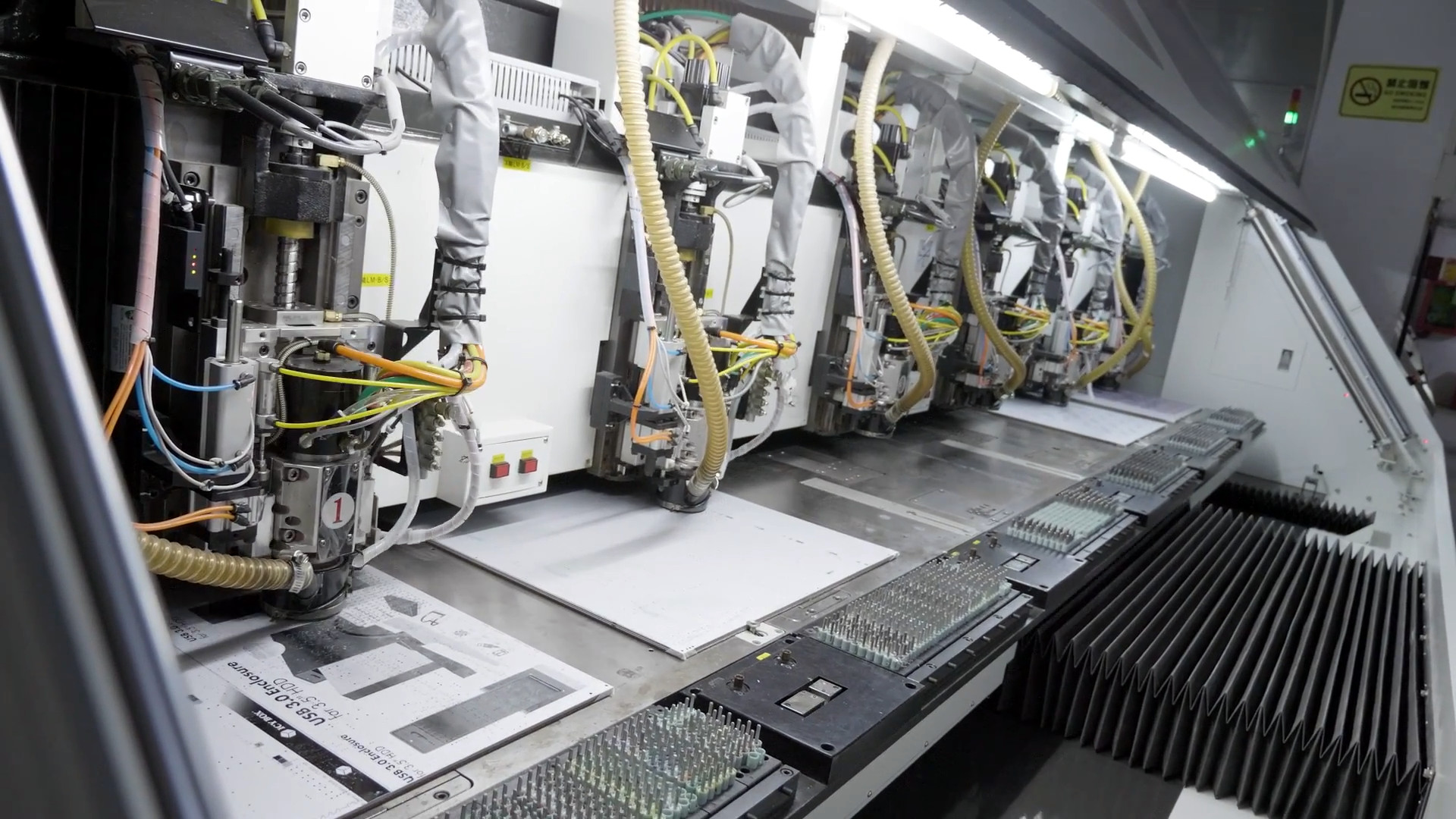
The drilling process isn’t so much a surprise as it is a marvel to see huge machines with six drill heads working on multiple boards at one time. It sure beats a Dremel drill press. The solder mask process is one that we don’t often see shown off. The ink for the mask is applied to the entire board and baked just to make it tacky. A photo process is then utilized which works much in the same way photoresist works for copper etching. Transparent film with patterns printed on it cures the solder mask that should stay, while the rest is washed away in the next step.
Boards continue through the process to get silk screen, surface treatment, and routing to separate individual boards from panels. Electrical testing is performed and the candy making PCB fab process is complete. From start to finish, seeing the consistency and speed of each step is very satisfying.
Looking to do a big run of boards? You may find [Brian Benchoff’s] panelization guide of interest.
Continue reading “Scotty Allen’s PCB Fab Tour Is Like Willy Wonka’s For Hardware Geeks”