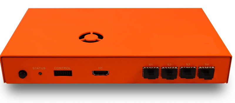
Got $4,000 to spend? Even if you don’t, keep reading — especially if you develop with FPGAs. Exostiv’s FPGA debugging setup costs around $4K although if you are in need of debugging a complex FPGA design and your time has any value, that might not be very expensive. Then again, most of us have a lot of trouble justifying a $4,000 piece of test gear. But we wanted to think about what Exostiv is doing and why we don’t see more of it. Traditionally, debugging FPGAs meant using JTAG and possibly some custom blocks that act like a logic analyzer and chew up real estate on your device. Exostiv also uses some of your device, but instead of building a JTAG-communicating logic analyzer it… well, here’s what their website says:
EXOSTIV IP uses the MGTs (Multi-Gigabit Transceivers) to flow captured data out of the FPGA to an external memory. EXOSTIV IP supports repeating captures of up to 32,768 internal nodes simultaneously at the FPGA’s speed of operation (16 data sets x 2,048 bits).
EXOSTIV IP provides dynamic multiplexer controls to capture even more data sets without the need to recompile. Dynamic ON/OFF controls of data sets let you select the data set and preserve the MGT’s bandwidth for when deeper captures of a reduced set of data is required.
In a nutshell, this means they use high-speed communications to send raw data to a box that has memory and connects back to a PC. That means they can store more data, have more data come out of the chip over a certain time frame, and do sophisticated processing. You can see a video about the device below, and there are more detailed videos on their channel, as well.
There are two things you might be wondering. First, why not just send the data to the PC instead of an intermediate box. Notice the box has a USB 3 connection back to the PC. That’s fast, but it isn’t fast enough.
The other thing you might be wondering is why you’ve read this far since your boards don’t have MGTs and you don’t have $4,000 sitting around to buy a debugging tool. But it occurs to us, that while the implementation of this idea is very robust-seeming, there’s no reason we couldn’t adapt it to our FPGA designs. Why haven’t we seen a hacker design that uses a reasonably cheap and fast I/O (maybe LVDS) to pipe data to an Arm board with some memory. In fact, you would think you could separate the modules for the FPGA so you’d have a core and a communication channel that would allow different features.
Of course, open source debug cores are not unheard of, but they tend to work like traditional JTAG debuggers where you essentially build a logic analyzer on the spare parts of your FPGA. We haven’t seen anything like the Exostiv solution. Probably the closest we’ve seen is this device from Cornell, but it displays on a VGA monitor. There’s also no shortage of standalone logic analyzers that use FPGAs.


While it is impressive it is also a lot of dosh, especially when you consider that we’ve all got used to bugs in almost everything and either ignore, reboot or circumnavigate the issue somehow.
It appears from your comment you are not working in that field of expertise. Simply know that clients usually expect their IPs to be bug-free, especially if they’re producing an ASIC or deploying a product in the field ????
Same in software, and like with hardware, client expectations are not physical realities, and in the end they involve blame more than achievements.
No misfeature will be called a bug, not even accidental misfeatures.
I mean, otherwise all the products that contain ASICs would be without bugs!
Lauterbach tools start at about ten times that much, but as always it’s the software and support that’s make-or-break.
Not 10x, a software licence is around 4k$ and hardware is 10/15k$ for a jtag/ETM probe
Meh. This is the sort of thing complex SoCs have been doing for at least a decade. Poke some internal registers, and get an 80MHz serial stream of internal state in our case.
$4,000 is justifiable for those who have a good business case. People wouldn’t blink if some one said we need a new company van.
Idk, my friend runs a company that transports steel from Poland to Ukrain. His entire fleet is made of early 1990s VW Transporters. By saving on company cars he could afford to buy a new Dacia Duster with cash.
https://www.youtube.com/watch?v=R1gbWpn7Ngc
Agreed that 4k is nothing when a single FPGA costs in the thousands. But the hard part is to justify the time that your engineers have to waste to get this up and running while providing negligible return on investment.
If you know what you are doing the up and running time is about 8hrs for one engineer. I’ve been lucky enough to have the opportunity to use it for debugging dram buffering for network streaming. It works, and the capture depth is a sine qua non for finding bugs in some designs.
How much did the mic that picks up your whining cost?
About half as much as the one that picks up whining about whining, because one less amplifier stage is needed, and you even don’t have to low-pass filter the virtue signaling!
But if you don’t have a whine filter, you could get into whine-whine heterodyne which has a good beat but ten to one you can’t dance to it.
I suppose the budget alternative for hobbyists would be a HDMI capture card or a FX3 card?
Budget alternative exists, if you develop with xilinx FPGA it’s called chipscope. Best of all it’s free.
But without that capacity is the point.
Dumb beyond belief. I thought long and hard what application this might fit in and in every case there are simpler, cheaper and faster way to debug.
Then this device is not for you. This is basically probes a large mount of the internal FPGA state concurrently and can be used for verification in design. For a market ready MCU with a CPU,like the ep8266 on your blog, the internal state is assumed fine and tested by the digital designers/verifiers and thus the functionality is only a function of your external device state/ IO pins and program code. Where the internal state is not okay in testing after production, say due to silicon bugs at the digital section even after correcting all bugs at the design stage…an errata document is supplied.
For simple bugs Xilinx has chipscope, albeit it’s relatively low speed and doesn’t have such a huge storage. For really nasty bugs designers typically put custom debug logic to capture relevant signals. For bugs related to FPGA routing / timing putting a tap for this device wouod certainly change the placement. Do you have an example of bug / design that could be debugged more effectively using this device?
Thanks for stopping by my blog btw.
Sure thing :)
I don’t think it would change the placement much as this would sample the voltage at the node in parallel arrangement. I would like if somebody could confirm this for me.
Of course test HDL should be similar to the actual HDL with the test framework in mind. The use case for this device is that it would be great for testing complex IP for sale/production, especially if the IP is meant to be used in safety critical systems.
I don’t think you have control over placement since it’s probabilistically optimized. Basically even if you only change a register name the placement could be completely different with the same synthesis seed, let alone putting a tap and route it to your serdes.
JTAG is typically used for post manufacturing test. Why would you waste serdes and board real estate for the qsfp plug rather than use the industry standard JTAG? If the reason is that you have to dump gigabits of data for each board during post manufacturing test then something else is very wrong!
I wonder what the breakdown of Hackaday readers is these days. It always seemed like it was just hobbyists and tinkerers. Is there a significant percentage of Hackaday readers who work in the industry and would find this post useful beyond an odd curiosity? If so, cool! Hackaday is all grown up. :D