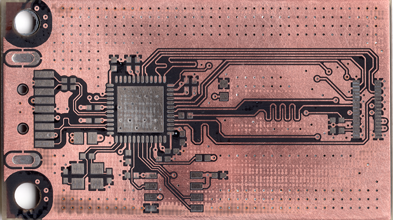
Every once in a while, and more so now than before, you’ll find a really neat chip with zero documentation. In [David]’s case, it’s a really cool USB 3.0 eMMC/ SD MMC controller. Use this chip, attach a USB port on one end, and some memory on the other, and you have a complete bridge. There are drivers, too. There are products shipping with this chip. The problem is, there is no data sheet. Wanting to use this chip, [David] turned to sandpaper to figure out the pinout of this chip.
The best example of a product that came with this chip is a simple board from the hardkernel store that happily came with fairly high resolution product photos. While waiting for these boards to be delivered, [David] traced the top layer of copper. This was enough to get an idea of what was going on, but the real work started when the boards arrived. These were placed in a flatbed scanner and carefully photographed.
The next step was to desolder all the parts, taking care to measure and catalog each component. Then, it’s off to sanding with 200 and 600 grit wet sandpaper. Slowly, the soldermask is removed and the top copper layer appears. After that, it’s just a matter of sanding and scanning, stacking all the layers together with your image processing software of choice.
There are a few caveats to hand-sanding a PCB to reverse-engineer the copper layers. First, it makes a mess. This is wet/dry sandpaper, though, and you can and should sand with water. Secondly, even pressure should be applied. We’re not sure if [David] was holding the sandpaper or not, but the best technique is to actually hold the board itself.
Despite a few problems, [David] did get the pictures of each copper layer. After assembling these images, he could make an Eagle part for an eMMC reader for his Nintendo Switch.


A short Google search gave me this schematic: http://image.cirmall.com/Fue7gNYf8jaEDJAz2uKquo15t173?watermark/1/image/aHR0cDovL2ltYWdlLmNpcm1hbGwuY29tL2Npcm1hbGwtd2F0ZXJtYXJrLnBuZw==/dissolve/50
Not EMMC, but SD, but enough to build your own device, I guess.
Ok, kudos for the effort as an excercise.
But there is a datasheet (As he states himself). All you possibly have to to is remove the SMD sprinkles to get their values?
The chip itself is an SD/eMMC reader depending on how it’s configured. This project was purely a pedagogical exercise. I had the schematic going into it which meant that I had the ideal baseline to compare my results to. I could have just used that data, or emailed the person on the front, but that would have defeated the learning experience.
A quick google search: http://img.hqew.com/file/Others/110000-119999/113018/Electronic/20158915512683924.pdf
Is that using SD/MMC’s SPI fallback mode?
I’m about 75% certain that is not available with eMMC.
(as to eMMC, the main challenge there is the fact that it’s usually a BGA soldered to whatever device it’s used in… Not any interface circuitry.)
The article mentions that the part is s a GL3224. That one knows how to handle eMMC in 8 bit mode.
The eMMC standard basically requires that the controller explicitly not support SPI. As for WHY they would do this, I don’t know – one would think that a storage device (that has “embedded” in the name nonetheless) should have SPI support so that even low-cost MCUs can use it easily…
Although eMMC is a pretty finicky 0.5mm pitch BGA package, they can be wired up manually. I turned one of mine into an SD-form factor card: https://ripitapart.com/2016/10/28/emmc-adventures-episode-1-building-my-own-64gb-memory-card-with-a-6-emmc-chip/
Sounds like a lot of effort to what could probably have done much faster with a continuity meter after having removed the components.
Surely that would really depende on the number of pads, the time taken would increase non linear with each additional pad on the board. e.g. 2 pads would require 1 test, 3 pads would require 3 tests, 4 pads would be 6 tests, 5 pads would be 10 tests, 6 would require 15,…
There is probably close to 100 pads on that board and that would take a while. You could reduce the testing in half by ignoring all pads that are clearly connected to ground.
e.g.
For 50 pads it would require 1225 continuity tests (50*49)/2
For 100 pads it would require 4950 continuity tests (100*99)/2
For 150 pads it would require 11175 continuity tests (150*149)/2
For 200 pads it would require 19900 continuity tests (200*199)/2
There is a point where using a continuity meter is just not worth the effort. The sanding down approach becomes attractive very fast as the number of pads increase.
Damn Son.
Not entirely true;if you have determined 2 or more pads are connected, you don’t need to test every other pad to those individually, you can consider them as one. Also, on such a board, except for the power nets. by far most nets will have 2 pads. Checking if a pad is connected to the single large IC is as simple as dragging the probe of a good multimeter (with a fast continuity buzzer) across the pins of the IC; you can hardly consider that separate tests.
Also, a signal can only go to and from the inner layers through a via, and the power and ground vias are easy to identify (power vias are usually close to a decoupling capacitor). Color-coding those with a marker leaves you with vias that need to be checked against other vias.
Both methods can work, if you have to luxury to sacrifice a board for destructive analysis, that would be less mind-numbing then spending hours with a multimeter and a notepad.
I agree with everything, my quick and dirty calculations were just back of the envelop style for a totally generic unknown board (without the application of any expert knowledge). But we both do agree that once it gets to a certain scale of pads it will just becomes a mind-numbingly boring process. And that is exactly when mistakes happen, the last thing you want to do is have to start again.
With a simple continuity test, there is also the possibility of totally missing things in a mixed signal high speed PCB with grey beard RF microwave black magic inside ( https://www.reddit.com/r/electronics/comments/2q2eeu/how_it_feels_like_trying_to_understand_rf_black/ ).
Right, you need to reduce the circuit by combining any pads that are interconnects down to single points. You will eliminate a ton of them this way since any PCB has a bunch of vcc and ground connections. However if the IC had a datasheet then there should be enough data to construct a device using the IC. After all someone designed this circuit in the first place and I would assume most IC manufacturers would like people to design around their devices.
52 pads on components
9 pads on the USB3 connector
34 pads on the eMMC connector
48 pads on the big chip
8 pads on the little chip
151 total.
I would call it a push, ohmmeter vs. sand’n’scan. I would probably go with the ohmmeter myself, since there’s still a great deal of manual work once you have the scans composited, i.e. you have to “measure” with your eyes to generate the netlist. I would use a sharpie to mark each pad that’s been accounted for, and start with grounds and Vdd, which would leave considerably less than 11,175 tests to be done.
Also, Truth, your math assumes that each pad connects to exactly one other pad, which is the worst case.
One disadvantage of the ohmmeter is that due to parts of the circuit operating in the GHz frequency range bits of the PCB are waveguides and you may miss some intricate details by just testing DC continuity. But if you are a grey beard RF engineer then you would just assume that all tracks are controlled-impedance lines of 50 ohm impedance, and design around that, most of the time you will be right but some high speed parts are not 50 ohms impedance.
Even just looking at the image above there are extra loops of track to keep the length (and impedance) exactly the same of some critical differential signal paths.
And possibly what may be a 5th order LC bandpass filter made out of PCB track.
By the way you pointed out that my quick and dirty back of the envelope style of calculation is for the absolute worse case, I do not see one thing wrong with a generic estimate. My main point has been and still is that the work required increases with each additional pad in a non linear way. So worst case or best case does not matter, the work required will still increase in a non linear fashion.
It’s not like a solder mask is hiding any of the copper underneath. The traces are very often (always?) easily visible without sanding or removing components. It would have to be a very strange board to have a solder mask that occluded the copper traces completely. That said, being able to see the traces gives a very easy target for the continuity tester. This board isn’t that complex. It should be easy to reverse engineer it without having to sand it or un-solder all the parts. I’ve done this countless times, it’s really not that as difficult as this guy thought, but maybe he’s inexperienced.
I wonder if one could intentionally cause the board to delaminate between the layers. Something like soaking in water for a few hours and then putting quickly to a hot oven.
Or similarly, chemically dissolve the epoxy.
Perhaps MEK or Methylene Chloride would do it?
I recently went looking for those two items. I occasionally use them in small engine fuel system repairs and other misc cleaning chores.
Big box stores in my area have stopped carrying MEK and Methylene Chloride.
According to what store employees told me: Meth/chlor, Seems too many idiots have asphyxiated themselves remolding bathrooms or whatever.
Then MEK is apparently presumed to be associated with drug production nowdays.
I have yet to check with any remaining, commercial paint stores for availability.
Better grab them if you can still find them.
I know I saw MEK a few years back, never used it for anything.
Methylene chloride (aka dichloromethane, similar to trichloromethane, aka chloroform, incidentally) I purchased (with some other ingredients) as paint stripper to weld acrylic. I actually wanted Weld-On, but that’s what I was able to find in a weekend.
I’m sure you can still get them commercially, but that’ll be a bummer if I can’t find them any more at Lowes.
Bright Blue Jim, I wasn’t expectng the fibers to go anywhere, but I honestly hadn’t thought about the problem of vias and plated through holes tying the layers together until you pointed it out. Perhaps the ideal method would weaken the interlayer bond to allow you to peel them, while leaving enough strength to not crumble in the process.
Sheesh. Looks like the thousands of us who, for many years, handled these things with reasonable bit of care, are now going to lose them due to a few Darwin candidates who refused to use a minor amount of common sense and a fan or a chemical rated mask.
https://www.mercurynews.com/2018/06/20/home-depot-lowes-to-cease-sales-of-chemical-blamed-in-accidental-deaths/
All it needs next is a “social media” campaign and the commercial stores may drop them.
Contrary to marketing claims, citrus based cleaners just flat out do not work worth a f### on petroleum residues and many adhesives or degraded/gummy plastic residues.
Yeah, Methylene Chloride should definitely be treated with care. Precautions should be taken to minimize any exposure, as it readily enters the blood stream through skin, lungs, eyes, etc. and can carry other chemicals/poisons with it. Gloves, safety glasses, respirator… If you don’t have a respirator, then at the very least use very small quantities in well ventilated areas. It’s very volatile and has a sweet smell. If you can smell it, the ventilation is not enough.
That said, its very good at welding acrylic, but you have Zero chance of repositioning the parts and it starts dissolving the acrylic immediately, so don’t get it anywhere but in the joint you intend to weld. Also, it doesn’t fill gaps at all, so you need to have clean cut smooth edges if you want to have a good looking and strong joint. I would use a very small needle applicator on a squeeze bottle. Capillary action is the name of the game.
Pro tip: Don’t fill the bottle up. Then you can squeeze the “air” out of the top before you tip the bottle over to dispense it. As you tip the bottle over, loosen your grip so it creates a vacuum and keeps it from squirting all over your part. You have much better control that way.
I remember Shank saying he tried this with a wii board, I think he said it worked but kinda messed up the other layers (I could be remembering wrong) I also think someone used a razor to peel layers of one apart, I don’t know how successful he was. But even though sanding is probably one of the more tedious methods, it’s incredibly effective if you’re careful & have a decent setup, there’s a good reason it’s one of the more common methods for reverse engineering boards. (Though leaking the internal design documents also works pretty well)
You’re still going to have problems, as the through-hole plating will tie all of the copper together, and of course, the glass fibers aren’t going anywhere.
If the chip is so poorly documented, how are companies using it? Do they only provide the datasheet to customers ordering more than n chips, or…?
Click on the linked article above and read the first two paragraphs for your answer.
Yup. And by the way, this is SOP for nearly anything Hardkernel sells. They seem to be the way that certain Asian companies can claim to have developer boards when, in reality, their products are poorly documented crap.
You know a company is doing a poor job of documentation when the BSP is a multigigabyte tarball download from the devboard vendor’s site. (For reference, compare to https://source.codeaurora.org/quic/la – Not that Qualcomm are angels in this regard by any means, however they’re leaps and bounds ahead of pretty much anyone else in the industry.)
Their support is fine if you approach them as a genuine company with a genuine need. I evaluated this part personally for a project and found it pretty good for the purpose. We ended up using another part, but not because of deficiencies in the GL3224.
Has anyone ever tried paint stripper or other dissolvants on a solder mask?
I need to read into this more… since I was wondering why there are no USB 3.0 chipset bridges say like for example using the FT60x or other chipsets that are under $10. There are Broadcom USB 3.0 to SATA that are even cheaper. Would be interesting to have a USB 3.0 bus pirate or even since the chips have the capabilities within looks like I2C, UART, etc. I the market supply still too high with the USB 2.0 so no one wants/needs to hack their devices to USB 3.0?