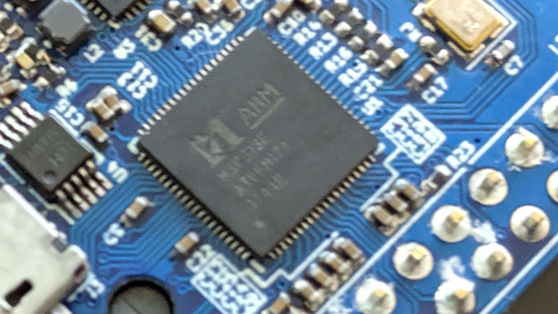
As the onward march of technology delivers ever more powerful semiconductors, it can be instructive to keep an eye on the periphery of the system-on-chip market for niche-application devices which may have an application in our sphere. Just such a chip is the Mstar MSC313E, a SoC designed for use in IP cameras that packs an ARM Cortex A7 and 64 MB of memory, 16 MB of flash, Ethernet, USB, and all the other usual interfaces you’d expect from a microprocessor. It’s available in a QFN package which makes it tantalisingly within the reach of the hardware hacker community, so naturally there is significant interest in unlocking its secrets. A cheap and accessible part with enough power to run a stripped-out GNU/Linux operating system has to be worth a second look!
QFNs are not the easiest packages to hand solder, but if you also find yourself in that position there is at least the prospect of a ready to go development board. The BreadBee is a small PCB that packs in the chip with all its interfaces including Ethernet and USB brought out for experimentation. If you don’t fancy building one, you don’t even have to: it’s soon to be crowdfunded.
One might ask what the point is of Yet Another Linux Capable Microcontroller Platform, given the plethora of Raspberry-pi and competitor boards. The answer to that is simple enough and contains within it the essence of hardware hacking: because it is there. We might never see it again save for in a few outlying projects, or perhaps it might find a niche in our world and become popular, without this early work we’ll never know. While we’re at it, this isn’t the first such SoC that’s emerged; we’ve previously seen an action cam chip give us a hand-solderable Linux single board computer.
Thanks [anonymouse] for the tip.


Nice if we can ditch spyware infested IP camera firmware and put on board motion enabled opensource firmware on them!
https://github.com/fifteenhex/mc200c2camerahacks
Hacks for the MC200C2 module available from Banggood.
To me those specs scream OpenWRT/LEDE. 16 Flash / 64 Ram is super common for many small simple router implementations. The only question becomes what did they use for Ethernet and such. That would be key if OpenWRT would run on it. Otherwise have to look at a Yocto type strip down.
Not sure what you are getting at for the Ethernet. It got 1 built-in Ethernet MAC + PHY.
So you can do a One-armed-router like most of the WRT routers by adding an external Ethernet Switch.
https://en.wikipedia.org/wiki/One-armed_router
The CPU is kind of weak – single core Cortex-A7 at 800MHz.
For the kind of extra things to get it run, you have better luck going to your Thrift store and find a better spec used router that can be hacked.
800MHz is quite a lot faster than what’s used in cheap routers. The venerable AR9331 is half that with a much older core.
Some of the cheap routers have hardware assists routing. e.g. CTF for NAT acceleration that helps to offload the CPU load.
You might be the only one that be porting to OpenWRT as it isn’t ready as a router as is. By the time you add a $5 Ethernet switch and figure out how to set up VLAN, port OpenWRT to this part, you are better off getting a $5 routers from a Thrift store. I have picked up $5 routers that can run Tomato firmware and one even has Gigabit LAN ports.
And that assist doesn’t help much as soon as you are doing something minimally non-trivial.
AR9331 is perfectly good to 100Mbit.
OpenWRT is still a fine distro for the hardware, you don’t *have* to use it as a router OS after all….
I am finally getting time to start an RPI Compute Module project. I want to make an integrated solution with a CSI interface, POE, internal SD/HDMI/USB, and a header for optional audio.
I think that a solution like this would be awesome with MotioneyeOS, and an audio suite for 2-way audio.
I figure that the extra heat that thing will produce will keep it thawed in my Canadian winters… :)
I mostly want to merge a security solution with a local smart-speaker solution for in-home and off-cloud smart home functions.
Tap into the speaker drivers for dynamic microphones.
google for the chip, but the unfore site requires some social network before showing SDK. Don’t bother as they don’t show link anyways – see comments
github under folder breadbee/breadbee – still work in progress, but should get you started with uboot, kernel and buldroot
http://linux-chenxing.org/ follow the rabit hole and *eventually* you’ll find a data brief with the electrical side under Infinity 3 link.
Seems to be a bigger version: MSC316DC – Cortex A7 + 128MB DDR3 in a QFN88
Woo, that’s an upgrade from DSL to Slackpuppy.
Really interesting little board. Signed up for the project, can’t wait to cowdfund
Can you get 5 hand solderable PCs off of ebay for $10?
5 of these chips are going for $10 on ebay at the moment.
I was going to say, that is the reason to play with them, generally once you have all the “stuff” on the lsi, the price goes down quickly. Yes, it may be watered down compared to an rpi, but for a real price of say $5 for a board, and with the price posed to go down as production scales up, that makes it appealing. The pi zero was $5 and a few folks even got them for that. Look at what they cost now. What is odd though is the cost of flushing a pi out has went way down, sd cards are dirt cheap, usb power supplies have plunged in price, but oddly the pi has maintained the same price point, though with better specs, or gotten even more expensive. It would be nice to have a $5 alternative poised to cost less in the future.
Tempting but can’t see myself building Pi Zero scratch from schematics to soldering to bringup
Dell almost exclusively uses mstar chips as monitor display driver ICs. They used to use st / genesis chips but I can imagine the penny pinch hammer kicked in. Dell probably doesn’t even design any part of their monitors anymore regardless. Havn’t seem a single datasheet or any document from an mstar display ic. Not sold at any legit vendor or distributor. Not worth the trouble to implement.
This seems like a decent chip and all.
But the picture for the article bugs me to be fair.
There is more than 1 capacitor that sits askew….
Starting from the top left corner, we first have an inductor and capacitor that aren’t properly on their pads and potentially touching… Then there is a capacitor right next to them that isn’t even sitting on its pad, but rather just floating there.
Then closer to the microprocessor itself, we have another pair of capacitors hugging each other.
Not to mention what looks like a 0201 or 0402 capacitor laying between two pads up at top center of the image… (hard to tell due to the blur, could be silk screen. But the other mistakes makes me doubt that.)
Then there is the rest of the board where few components seems to be placed all that well.
The amount of solder varies like crazy, so obviously hand soldered. (Nothing wrong with hand soldering, but at least get the components to where they should be….)
This board doesn’t pass my QC check….
>Then there is the rest of the board where few components seems to be placed all that well.
>The amount of solder varies like crazy, so obviously hand soldered.
The solder mask on the first boards was really bad. You can actually see near the top that the solder mask is so bad the track between two components is exposed. These were built up with hot air, solder paste and a toothpick.
>This board doesn’t pass my QC check….
It’s sort of a shame that every one I’ve made works then really.
Anyhow, this was the whole point. With integration at this level you can embed a relatively quick and cheap system with post 1980s features like memory protection onto the cheapest boards with horrible solder mask from JLCPCB with so so soldering.
QC isn’t just validating if something works or not. But also about mitigating future issues. And ensuring that everything is where it is supposed to be. Some of these components aren’t even on their pads.
Another part about QC is about ensuring that it looks proper. It helps future servicing of the device, and generally instills better confidence into the end user.
That a pair of components/leads are touching/bridging isn’t always wrong, sometimes there frankly isn’t room to do things another way. But on this board, there doesn’t seem to be much excuse. The components could have been placed a tiny bit further away from each other to ensure that the components stay on their own pads.
QC is “quality control”, not “functional test”, the later on the other hand would only fail if the product doesn’t work as intended.
This particular board could be optimized to solve all these issues. So I wouldn’t really blame JLCpcb for people not following their recommended guidelines for the solder mask. (Increase the component spacing just a tiny bit, and the problems will go away. Can also move towards larger passive components, they are easier to solder.)
But the project idea is still rather nice and useful. I can see a lot of applications for such a board.
>QC is “quality control”, not “functional test”,
My QC process is: Solder it, check with a microscope that components are electrically mis-connected, rework if needed, check the power supplies… use it.
>the later on the other hand would only fail if the product doesn’t work as intended.
This board wasn’t a product. It was a prototype.
>This particular board could be optimized to solve all these issues.
It’s almost as if the board pictured was a prototype and the issues with the solder mask etc are fixed already. Really if you’re going to try and pick holes here go and look at the original gerbers where I messed up the pad size for one whole edge of the main QFN and didn’t spot it (thought it was JLCPCBs renderer doing something weird with half pixels).. however the boards still worked.
>So I wouldn’t really blame JLCpcb for people not following their recommended guidelines
Eh no. The JLCPCB silkscreen was awful for this board. Same gerbers produced by Pcbway was far better. However the JLCPCB boards were good enough. The boards worked first revision, first PCB run.
>Increase the component spacing just a tiny bit, and the problems will go away.
I’m not sure if you took five seconds to take a look or not but there isn’t much space to move stuff around will trying to keep the track/space 6/6 so it can be made super cheaply.
>Can also move towards larger passive components, they are easier to solder.)
Again, there isn’t much space. 0603 would be easier to solder but you aren’t going have a board that small once you do that. 0402 is not insanely small, possible to do by hand and not one of those really tiny sizes where the component cost goes up.
>But the project idea is still rather nice and useful. I can see a lot of applications for such a board.
The project isn’t really the board. The project is: Here is a complete, modern-ish processor that can run a recent linux kernel, python etc that is cheap, can be used in almost any project if you can manage to get 3 supply rails working and isn’t a BGA.
Prototyping is one thing, there QC is that it works. (The board can even have problems rendering some of its functionality broken. Unless one does a production sample then it should be what one expects from production.)
In production QC is far more than just testing basic functionality.
Now, I speak from the perspective of production. (Since that is my line of work.)
I am simply saying that this board has numerous quality issues and that it doesn’t pass my fairly basic quality requirements. (I am not even going that far in terms of QC either, just that the components should be on their respective pads)
Secondly, I haven’t studied up on the project, not checked any gerbers and the like, especially not gone through the project history. Have though prodded the links a bit. I simply shared my two cents on a bunch of mistakes in a picture of a board.
I came in with the perspective that this in fact were a picture of an “off the shelf” product. And with that perspective, this board is poorly put together.
That it’s actually a picture of a very early, if not first prototype is changing the perspective. But that doesn’t change my argument that this specific board is still having fairly poor quality. You don’t need to defend your fist mistake riddled prototype, we all make such prototypes.
(And talking about poking holes in things, at work I have seen prototypes with actual holes drilled in them. So that one can jumper wires from one side to the other. Your board at least isn’t having such issues. (Also, as a piece of advice for people doing larger more complicated boards (for small production runs/prototypes), having a hole or two for this very reason on the board can be a very nice touch, and can save one tons of time and money.))
>I came in with the perspective that this in fact were a picture of an “off the shelf” product.
This is hackaday which generally isn’t about perfect off the shelf products.
>You don’t need to defend your fist mistake riddled prototype,
There is one issue with the solder mask which is easily resolved by ordering boards from oshpark or pcbway. Functionally it works fine.
You’ve made an assumption that the photo is of a production machine assembled board and gone off the deep end about QC.
Do you ever get that feeling just before you click “Post Comment” when you wonder if you should just delete the comment and go about your merry way? Trust that feeling. Be merry.
Yes, something that thought does cross my mind.
Sometimes I skip a comment.
Other times things are just worth while pointing out.
Part of the design rule to watch for is the minimum solder mask width. If you fall below that, they might remove the solder mask between the two pads and your components hug each other due to surface tension. Functionality might not matter, but it can become a yield and long term reliability issue.
>Part of the design rule to watch for is the minimum solder mask width.
I don’t remember entirely but I think the first gerbers met the those rules. The solder mask was present in a lot of places initially but the adhesion was bad or something because it started peeling back just from soldering. From my experience JLCPCBs soldermask and silkscreen just aren’t that good but you can’t beat the price for 10 boards. Once you’re making thousands of boards using pcbway instead doesn’t affect the price anymore and it’s my intention to use something better than jlcpcbs cheapest service for the crowdsupply boards.
>Functionality might not matter, but it can become a yield and long term reliability issue.
Yep. But that was a prototype. If I was concerned about long term yield and reliability there I wouldn’t have soldered it with lower temperature solder, used the cheapest PCB service from pcbshopper, would have cleaned off the flux residues around the 2.54mm header and so on. That board was built over a year ago now and was a PoC more than anything.
In my experience JLCPCB soldermask is fine for parts this size… you do however need to tighen up the mask if say you are using KiCAD make the mask clearance and min width fairly small… otherwise there won’t be enough mask between the pins for it to even exist… basically you don’t need any clearance.
>basically you don’t need any clearance.
Exactly. The fix was to just tweak the kicad settings to 0 so the mask was everywhere. I’ve started doing this for all boards and they’ve come back fine from jlcpcb and oshpark so I’ll probably keep doing that.
Either way the boards still worked. They were tricky to solder but I wasn’t going to throw them out to keep someone happy over the ins and outs of QC of prototypes for a little hobby project.
The SoC does not contain flash memory. It has to be added externally which is done on breadbee board (via SPI NOR).
People need to stop worrying and learn to love the QFN. If you must hand solder using long pads makes it easy to solder. If you use hot air, reflow, or hot plate then it’s one of the easier components to solder.
I can get a much more powerful all in one package from an old smartphone rooty tooted so not much need for this chunk.
Considering how much trouble the PostmarketOS folks have it does not sound easy or simple.
And what if you need hardware Ethernet and SPI?
Add to that the unfortunate fact that used cellphones are not something you can buy 1000units for some small product and get the exact same thing for <5usd/pcs.
I always see mentions about used cellphones being cheap and powerful, but i never see anything built with them.
Not even something like a pihole.
Yup, the difference between a hit and run “booted linux” and a functional linux system is more like continents than miles.
That is a lot of suppositions there. That chunk is clearly a better fit for your project that you need 1000 of and ethernet (though there are OTG adapters that handle that). Use the best tool that works for you :)
I have a lot of old cell phones that I use for things, but and this is a bit but, I am lazy and I just run dedicated apps that have alrady been written. I have one phone that I use with my guitar. It has a sensitive mic and the guitar tuning app I use runs great on it, I also have a metrome app and a beat box app that run well on it. No need to really hack anything. I have a couple other cell phones that I use as wireless cameras. Again, just running an app. No need to dig in any deeper. I have one out in the shop that has a couple programs on it for working with wood and what not, oh and the inclanometer, again canned. I live in an area without cell service and I have an old phone I take out for walks with me. I have tunes, and audiobooks, and it is handy having a camera. I don’t have to worry about dropping my good phone. I have at least one other phone that has a time lapse program on it. Agian, canned. So, old phones, and I am always picking up old phones, have a lot of uses. It would be cool to dig in a bit more under the hood, but really, why bother when most of what you want is already plug and play?
If a smart phone works for your project then I would say use that. The main issue I see is that you have to connect everything via usb unless you can work out where i2c, spi etc are broken out on the board. Your chances of getting a recent kernel are pretty low too.
If you just want a cheap board with ethernet then I would go for the rock pi s.
If you want a weird little board with a weird unknown soc that was reversed engineered by randomly pulling pins down to ground then I have you covered.
The project looks very interesting. Sad the camera can only to 30fps, but still worth to explore.
There was a similar project by Omega called Onion2, it was ~400MHz MIPS with 64MB RAM. Quite useable. This looks even better.
I’ve been waiting for someone to get one of these emulating some 1980’s micro. https://hackaday.com/2018/08/22/fcc-filing-reveals-tasty-hardware-mcsecrets
Hmm, interesting post thanks and also nice to see some thoughtful comments, cheers
Looks interesting. One question important for me: can I put it to sleep mode? It’s a thing that is impossible (Raspberry Pi, all OpenWRT boards) or unrelliable (Allwinner H3, H6 etc) on most of popular SBCs. And with sleep mode we can build range of great battery powered small linux devices!
Sleep mode should be possible as I have the vendor code that does it. It seems to support wake up from a GPIO, RTC, LAN or IR command event. The code basically sets up some values for the return and then turns the ARM core power off via a GPIO. The current board doesn’t support turning off that rail but I think it would be a pretty small modification to make it work. Alternatively maybe disabling the clock for the CPU would work. I would guess/hope it gets reenabled as part of the resume process.
Is it published anywhere? You having it is useless for the rest of us.
It’ll be published and integrated into the schematic once I work it out.
I look forward to seeing this mediocre little chip added to the roster of usable cheap SOCs. Thanks for the effort!