Join us on Wednesday, November 10 at noon Pacific for the Heavy Copper PCBs Hack Chat with Mark Hughes and Greg Ziraldo!
For as useful as printed circuit boards are, they do seem a little flimsy at times. With nothing but a thin layer — or six — of metal on the board, and ultra-fine traces that have to fit between a dense forest of pads and vias, the current carrying capacity of the copper on most PCBs is somewhat limited. That’s OK in most cases, especially where logic-level and small-signal currents are concerned. But what happens when you really need to turn up the juice on a PCB?
Enter the world of heavy-copper PCBs, where the copper is sometimes as thick as the board substrate itself. Traces that are as physically chunky as these come with all sorts of challenges, from thermal and electrical considerations to potential manufacturing problems. To help us sort through all these issues, Mark and Greg will stop by the Hack Chat. They both work at quick-turn PCB assembly company Advanced Assembly, Mark as Research Director and Greg as Senior Director of Operations. They know the ins and outs of heavy-copper PCB designs, and they’ll share the wealth with us.
 Our Hack Chats are live community events in the Hackaday.io Hack Chat group messaging. This week we’ll be sitting down on Wednesday, November 10 at 12:00 PM Pacific time. If time zones have you tied up, we have a handy time zone converter.


Huh. I had never realized that these were a thing. I mean, in hindsight it’s obvious that they’d be a thing, but it’s just not something that had ever occurred to me.
I can’t help but to wonder if the use of more traditional bus bars aren’t a better solution in some applications.
I have seen some PCBs using copper strips with the occasional strategically placed leg that is soldered in as any other through hole component.
Another question is if one could just add a layer of photoresist to a board, and simply selectively electroplate more copper where desired. however, this might not add any major amounts and would lead to height variations on the board. (as if that weren’t a problem with the board showcased in the article above.)
I have though also wondered about the possibility of getting better aspect ratio if one takes the etching in two or more steps. Re-adding the photoresist each time as to also protect the newly formed walls from further etching. (The board in the picture above seems to suffer a fair bit from over-etching in a few areas.)
Indeed, large bus-bars are often just hot-dipped water-jet cut plates, hydraulically crimped cables, and bolted together on a sheet of ceramic or flame-resistant glass composite.
Even just a 12″ wide 2oz PCB can be a nightmare to mix SMD parts on, as the bonded layers with dissimilar expansion coefficients form a bimorph cantilever. A conservative re-flow profile won’t help much given the stress from temperature changes often damages components, as the PCB badly warps if not bolted down (hence the same fastener fun as a bus bar).
YMMV ;-)
Years ago I worked for Sylvania Control Devices in Standish, Maine. We made millions of glass enclosed circuit breakers that were embedded in motor windings for over-current and over-temp protection, To test these and to check the distribution of production parameters we could develop a histogram. The breakers were immersed in a hot oil bath with the leads touching copper lands that were connected to an incandescent bulb. The operator would closely watch the lamps as the lights went out with rising temperature and relight when the temp was dropped.
We needed more of these 12″ x 14″ boards so instead of manually fastening machined copper pieces to the base, I decided to try a heavy G10 1/4″ thick board coated with 10 ounce copper. It took a while to find a supplier but I then silk-screened the desired pattern, drilled the board to just below the copper layer and mounted LEDs instead of filament bulbs. These worked great. This was also one of the first application of LEDs I tried. They were pretty pathetic compared to the current offerings but were barely bright enough. The pattern was large enough that the variations in etching wasn’t a problem.
It was a messy operation at best but the new boards being lighter weight made it a bit easier. Hard to believe that this was almost 60 years ago. Fond memories of one of the best jobs I’ve had among many others.
So, a very early adopter indeed. The first commercially-available visible LEDs I saw came out in the early 70s. They were horrifically expensive but plummeted in price mid-decade. Soon after that people started to think digital watches were a pretty neat idea.
We did a board that we were convinced needed 12 ounce copper on half of it (including the QFN package that was switching the 30A load) and the other half only needed 2 ounce.
It was a horrible experience. They did their best but we had shorts between pads on the QFN because the aspect ratio was so high, the plating wasn’t quite even enough to consistently get all 44 pads on the QFN soldered with no-lead solder (and finding opens on a QFN is a hassle) and reworking it was just wretched.
They did something like what you’re talking about, where they used 2oz foil and then plated half of it up to 12.
Since then we’ve used some combination of thermalcore daughterboards (for heat) and massively wide traces (for pure current) on our subsequent projects, and as we’re the chip designers, and realize other people will face the same issue, when we do stuff that needs this kind of layout we make sure the chip bond-out pattern allows for the required current in 2 ounce copper.
That is actually nice of you to ensure that it works in 2 ounce copper.
And yes, selectively adding extra thickness isn’t a flawless process in the slightest, though depends on the process.
I myself tend to use more than one layer when the current gets high enough if space is constrained. Not that this is isn’t brining in its own can of worms…
Sometimes it can be fairly nice to divide the board in two completely separate boards. One for all the large pin pitch high current stuff, and one for the high density logic stuff.
I know this way of thinking has its own flaws… but in this case I believe that if super thick etched traces were the best way to do things, it would already be common in industry.
Bus bars would be cheaper and easier to manufacture. Those chunky traces doo look cool though.
Looks like one could make a marble game out of that board.
That would be one horrifying game of marble, assuming power was pumped through it and the marble made of something like a ball barring.
That PCB looks weird.
It looks like that with half the copper thickness but wider tracks a very similar result could have been achieved.
It also looks like not much consideration is given to different currents going to different parts on the PCB. For some parts voltage drop is a concern, while for other parts just the current handling capability is important. Take for example a track going to a resistor.
Wider traces might not have been an option. If your power electronics are operating at mains voltages then the safety standards dictate reasonably large minimum spacing between traces (usually a few mm, depending on the voltage and what insulating material is present). Doubling the width of the traces might make routing much harder because, for example, you suddenly can’t get a trace between the pads of a standard through hole resistor and meet the minimum clearance.
It could just be bad design, but I wouldn’t jump to that conclusion based on the picture above.
On regular boards, they would mill out slots separating tracks that need more clearance. Not sure what the rules are for these types of PCB when you’ll also get I2R heating effects. At the very least, the tracks could be routed on the opposite layers instead so that wider tracks could be used – less heating effects, more adhesion.
Milled slots help with *creepage* but not *clearance* distances, and safety standards specify both.
I recognize that picture!
For context: https://www.reddit.com/r/electronics/comments/5i9wxd/i_just_received_my_20_ounce_pcb_soldering_is/ & https://www.reddit.com/r/electronics/comments/5urt3l/remember_that_20oz_700um_pcb_i_made_yesterday_i/
Thank you very much for that.
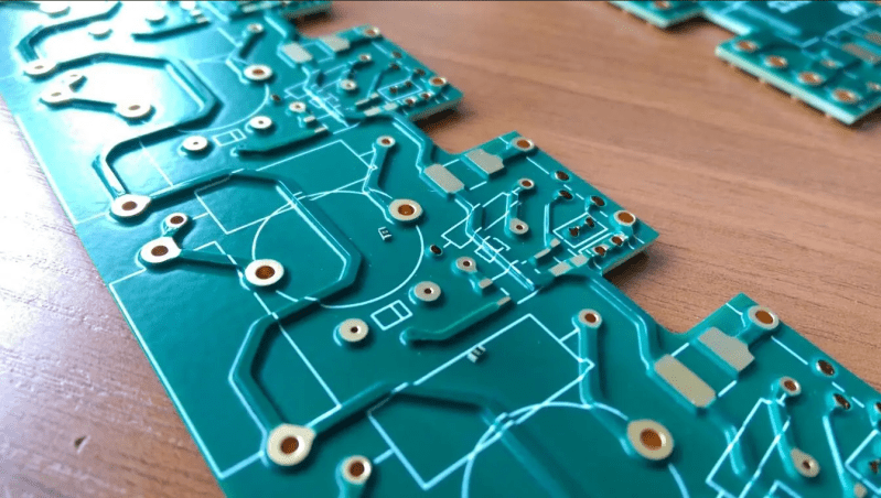
A summary of the PCB:
It’s a power supply for https://en.wikipedia.org/wiki/Formula_E
The bare PCB apparently cost USD 2250 to make, and that was considered “peanuts”.
The side shown has + / – 450V input, and the other side has 14V @ 150A and 24V @ 80A output and has 2cm wide tracks. That is 4kW and around 5A for the 900V side tracks.
(Or there are two for these PCB’s, one for 14V @ 150A and the other for 24V @ 80A )
Copper is 20oz (0.7mm) thick.
The SMT resistors shown for reference are 0603.
I was bonding this type of board at around 2012, 6oz copper then plating up to produce a thermally conductive double sided copper clad laminate to be processed as pth cappers and then bonded onto heavy copper panels and processed as a pcb, then finally milled and profiled. I have since wondered whether heavier copper track work could be cnc profiled and then tooled then bonded directly onto metal substrates using a thermally conductive prepared. This would negate the stepped etching problem.
With that kind of copper thickness casting it in a mold and then gluing some backplate to it is probably more efficient.
Quite some time ago there was a project with a 3D printer here which was modified to lay inductor from copper wires on a glue bed. That is a method that can be used to make custom PCB’s with thick copper.
With all those electric cars in these last few years (and all need electronics to drive their motors) heavy copper PCB’s are becoming much more of a mass product than it used to be.
Products like the PCB at the top of this article may be nice for prototypes, but the price tag is completely ridiculous for any product that is beyond the prototype stage. Just adding the copper by electrolysis probably takes several hours for such an amount of copper. Even regardless of the price it just is not feasible for mass production.
Etching PCB’s and plating works quite well for thin layers of copper, but thicker copper is badly in need of a more efficient production method.
“electrolysis probably takes several hours for such an amount of copper. Even regardless of the price it just is not feasible for mass production.”
Hmm. Yes, Faraday is a harsh master, but maybe thought-check that statement. The current price for copper is $10,000/ton. Current price for aluminum is $2600/ton.
And how is aluminum made again? Yep, electrolysis.
Those two are hardly comparable.
Electrolysis of copper PCB’s is done carefully in a bath of electrolyte.
Electrolysis of aluminum is done with the Hall-Herault proecess
https://en.wikipedia.org/wiki/Hall%E2%80%93H%C3%A9roult_process
It’s on a much larger scale and fine control is not needed, as the end result of that product is just liquid aluminum.
I do confess though that I have not done research on this.
During the plating process of via’s the copper is thickened from 17 um to 35um If you find a time reference for that and muliply it with 40 you probably have a somewhat accurate number
Just use copper heat pipes instead of copper traces ;P
Don’t forget the effect of skin depth: Past a few hundred kHz, adding thickness to a trace doesn’t buy you any more conductivity. You need to add width (or Litz techniques) to get more conductivity.
We used to manufacture products that switched fairly high AC current. Our Engineer’s solution was to design a double sided PCBs with standard 1 ounce copper and then plate up the current carrying paths. The designs worked really well but the switching relays and terminal posts had to be hand soldered in. The wider and plated up traces plus the metal inside the 30 Amp relays were too much of a heat sink to be reliably wave soldered.