This project, sent in by [Henk], goes through a few different ways to make a solder stencil using a vinyl cutter, a CO2 laser, and a fiber laser.
The project starts with identifying a method to convert the board’s Gerber files to a PNG, which is ultimately used to create a vector file for use with the laser. The first stencil, made with the CO2 laser, was cut out of masking tape. This worked fine for larger cutouts and is certainly a cheap option if you don’t have too many small components. A slightly better approach with the CO2 laser was using vinyl sheet release paper, which seemed to hold together better than the tape.

A vinyl cutter was also used as an experiment, but it didn’t perform as well as the CO2 laser, as expected, since the cutter uses a knife rather than light, leading to some tearing issues.
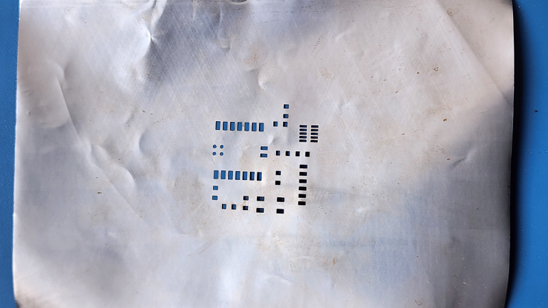
The final method utilized a fiber laser and an empty drink can to create a metal stencil. First, the can had to be cut open, heated, and flattened. The fiber laser was able to cut clean footprints in the aluminum, creating a stencil that would hold up to more use than the paper variations.
The finale of this exploration into laser stencil making was using the fiber laser to solder the board together. The stencil was used to spread paste on the pads, parts were placed on the board, and then the fiber laser heated the solder paste to solder them to the board. The board looked a bit toasty afterwards, but we imagine the process could be fine-tuned to reduce the collateral damage a bit.
Once you’ve got your stencil ready to go, you can combine it with a 3D printed jig to hold the PCB while you apply the solder paste.


Or just have JLC make it as well for $7 extra…
Or YoU cOuLD jUsT bUy iT
Hot take homie.
You are correct in the statement the stencils are quite inexpensive, there is a lot of value in making something yourself. If it isn’t for the skill, you may do so for your own satisfaction. Being able to do something yourself is of huge value, and creating a functional circuit board in literal hours is a huge asset in rapid prototyping. The OP uses both factory and self milled/etched boards.
I would be quite reluctant to outsource my hobbies, especially the parts which I enjoy. It is difficult to convey why I wouldn’t want everything automatic. Even very useful tools like 3D printers take away a from of the satisfaction of building something with your own hands.
Sure. But as someone who’s tried laser cutting a stencil at home (CO2), I don’t think it’s really worth it most of the time.
If you’re doing anything with 0402 or 0603 components or smaller, it’s near impossible to get a cut clean enough on a CO2 laser to make a decent stencil. Sounds like a vinyl cutter was even worse.
Having to spend a bunch of extra time reworking a board because I used a crappy homemade stencil (instead of just getting one made along with my PCB) doesn’t sound like the sort of joy you can usually expect from prototyping.
This work is done in a Fablab, which goal is to do it yourself. And to document so others can learn from your work.
Of course you can order cheap and have it shipped, but where’s the fun in that?
No matter how fast JLC is, they won’t be able to get it to me today, which is when I need it.
That might be due to subpar planning…
I know for myself that that’s the reason. :)
Basically electronics is a hobby for me and it should give me fun and satisfaction, and not stress. So I vibe my way through. Planning is for my job, where I get payed for stress and efficiency.
It’s not subpar planning if you did the design this morning, and fabricated the board using the same laser, by engraving a mask on the copper and etching it, or engraving the copper directly with the fiber laser.
I’m planning to do some experiments to create vias with the fiber laser, and engraving or selectively curing solder resist. The final step would be the ability to make solder stencils.
I’ve had some good results with regular printer paper for single-use solder stencils.
I’ve cut stencils on K40 CO2 laser out of sticker backing paper (slippery on one side, I assume silicone coated). It works great for one-offs down to 0.8 mm pitch chips.
I have done it with the vinyl cutter and super thin plastic, it helps to make the paste layer not have sharp corners, and dont use anything with fibers or you get the result showm (which is really bad in the article even for paper, maybe the bearing on your blade is clogged)
I shall have to remember this. I have a project where I need a stencil for an IC to fit in a rather tight space (rework). I lack a laser cutter, but I’ve got a vinyl cutter.
Unless it’s bga there is no benefit to using stencil/reflow oven.Just learn how to solder vqfn chips are very solderable by hand. By the time you mess with stencil, paste and removing anything that will melt from hot air/infrared/reflow oven I will have that vqfn100 chip soldered
If you are making five boards with twenty components each, a stencil and hot plate is great. You can do it a fine tipped iron and a steady hand, but it will take longer.
I somewhat agree, for one off’s its fine, when your doing a few hundreds of units its a huge time save
The workflow seems overly complicated – he converts the Gerber files to PNG, and then traces the PNG in Inkscape to get an SVG. It is much simpler to export the solder mask layer as SVG in e.g. KiCad.
This! The Gerber file is already a vector file!
It’s not only overly complicated. It also introduces needless conversion errors. So it’s more work to create a worse end result. But with all due respect. About half the people have an IQ that is below average.
I quite often point out (obvious to me) errors, and get a lot of flak for it. But my intentions are good. I’m hoping that people pick it up an learn something from it.
That’s just mean, I think the word you are looking for is median.
If you believe the current psycho-babble, human mental capacity has a normal distribution; hence mean and median will be the same.
Based on my experience, I am inclined to believe that the distribution is multi-modal. I suspect there are peaks about a sigma to the left, and about a half sigma to the right. Of course, I have no data to support my wild-ass suppositions (I should have been a politician).
Is actually a chi-square distribution not exactly normal. So median and mean are different. :-) probably not in any relevant way though.
I have used laser printable OHP transparency film and a CO2 laser cutter to achieve very good results.
Would maybe 3d printing a stencil work since you can print it quite thin
Or just solder it by hand, anything but bga and 50+ PCBs 20+ components each you will solder faster than you make the stencil. By time you mess with perfecting paste application method and fine tune owev settings you can make solder 40+ pcb’s by hand.
Do beer cans work better then soda cans?
https://hackaday.com/2013/06/14/machining-beer-can-solder-stencils/
https://hackaday.com/2013/02/04/diy-solder-stencils-from-soda-cans/
(And there are quite a lot more ways on hackaday to make solder stencils).
Uh, has anyone tried round pads? That might be a lot easier to produce. I suppose the pads might need to be a little bigger than rectangles, but that should be fine for a lot of projects that aren’t trying to be as small as possible.
as stated above if I use a vinyl cutter I go in the paste layers and round the corners. Least in Altium you can do a select similar objects, select options in PCB navigator (IE Layers and whatnot) and turn them all into rounded rectangles with a few clicks
Rounded corners is also an IPC recommendation. In engineering, square inner corners do not exist. there will always be some radius, such as from the thickness of the laser beam. Rounded corners also result in better paste release, and thus a more uniform amount of paste deposited on the pads.
KiCad is also transitioning to pads with rounded corners, and a lot of KiCad’s default footprint libraries already have rounded corners.
I have made numerous stencils the past ~10 years on a 2012 Epilog Legend 75 watt laser. I use 3, 4, and 5 mil kapton film from Amazon and raster etch the paste layer directly to the laser from a gerber viewer. (GC-Prevue and Viewmate both work well) The advantage of the Epilog is that the laser driver works just like a printer driver, so no need for any middleman NG/SVG/etc. I can etch from ANY program that can print in Windows. (I etched my resume onto a piece of acrylic directly from Word to show a colleague)
Kapton Tape works great from my experience.
I’ve managed to make some pretty detailed stencils (0603 and some fine pitched ICs) with alumninium drinks can using toner transfer. Reckon I could get down to 0402 fine. Cleaning the can first is the worst part. But cooking them on full in a pressure cooker for 10-20 minutes softens the print enough to wipe off with acetone. The laquer on the inside of the can can be a bit more of a challenge though.
Anyway – in case anyone wants to try –
1) clean cans
2) cut open and flatten
3) print negative toner print of component pads
4) iron onto clean(est) side of can
5) cover the other side with kapton tape
6) bathe in a 50/50 salt/copper sulphate bath (dissolved in water – exact amount of water I’d need to look into).
7) Regularly brush with a paintbrush during etching to remove the copper that’s deposited when the aluminium displaces it in the solution
8) rinse and peel of the kapton tape.
It’s easy to over-etch – need to keep a close eye.