Microcontroller addict [Debraj] decided to make his own programmable sine wave generator, and was able to put it together for under $40 USD. Other than low-cost, his list of requirements was as follows:
- Dual sine wave output, synchronized
- Frequency, Amplitude, and Phase control
- Low harmonics under 1 MHz
- Scriptable via Python
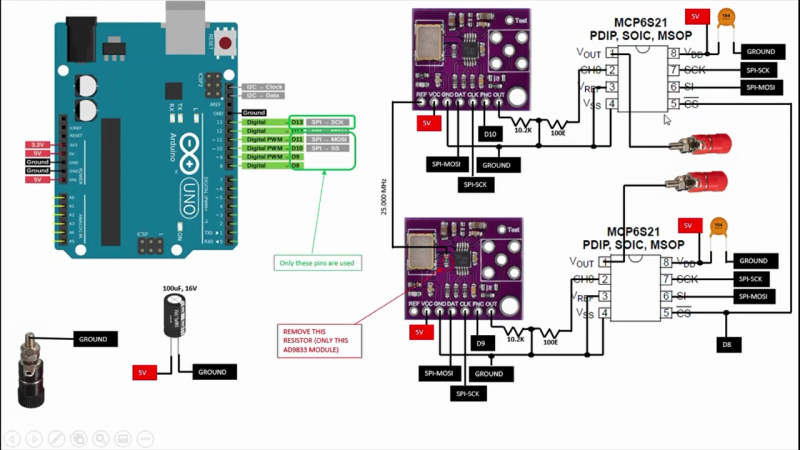
The heart of the project is the Analog Devices AD9833, a complete Direct Digital Synthesis (DDS) waveform generator system on a chip. If you’ve ever rolled your own DDS using discrete ICs or in an FPGA, you can appreciate the benefit of squeezing the phase accumulator, sine lookup table, DAC, and control logic all into a single ten-pin package. [Debraj] uses AD9833 modules from the usual online vendors for a few dollars each. He synchronizes the generators by disconnecting the reference crystal on the second module and driving it from the first one. The remaining specifications are met by the inherent characteristics of the DDS system, and the scriptable interface is accomplished with an Arduino controlling the AD9833 chips and two programmable gain amplifiers (MCP6S31). We like the confidence that [Debraj] displays by sketching the initial circuit diagram with a ball-point pen — check out the sketch and the final pictorial schematic in the video below the break.
This is a good example of combining off-the-shelf modules to quickly build a project. This approach is great for one-off builds or as a proof-of-concept test bed that can later be spun onto a custom PCB. Another reason to use modules these days is that the modules are often in-stock but the chips are unobtainable. Though it appears [Debraj]’s only needs one of these generators, it would be an easy board to layout and build — if you can buy the parts.


Nice tip, synching the XTAL that way. I doubt it´s possible to sync more than two devices that way without a complementary stage/buffer and i´m a bit surprised it works at all that way.
It works because it’s not a crystal (2 pins), it’s an oscillator (4 pins), so it’s a lot less fragile to line capacitance variations.
There appears to be no way to specify the relative phase, eliminating most of the utility of running the two off the same frequency reference.
And only good to about 1 MHz (though realistically, this is still usable to a few MHz with modest filtering).
If a broadband tunable sinewave is not an absolute need, the Si5351 will happily put out two or three unique frequencies from 8 kHz to well over 100 MHz, and guarantee the phase relationship too. (Also available in 8-output versions.)
The Si5351 does indeed output multiple output frequencies at the same time, but they are all square waves (pulses). Not helpful if you’re looking for sine waves.
The relative phases of the two 9833’s (at 1MHz) are coded in the Arduino code. A small phase shift between the 25MHz clock inputs still means the frequencies are the same (as long as the slaved 9833 doesn’t trigger on waveform ringing). A small resistance placed in the Reference clock circuit in series to the slaved 9833 would largely address ringing at the expense of increasing phase shift slightly. Replacing the jumper on the master with a similar resistance would correct that shift.
“We like the confidence that [Debraj] displays by sketching the initial circuit diagram with a ball-point pen — check out the sketch and the final pictorial schematic in the video below the break.”
Hehe. The final schematic (at 6:15) is different from the sketch in an important way, and won’t actually work :-)
There’s really only 2 minor differences between the circuits: 1) resistor dividers out of the AD9833’s (trivial), and 2) FNC outputs from the AD9833’s are fed back to the Arduino D8 and D9 (may or may not be an issue, depending on how the Arduino uses those pins).
More significantly, I don’t remember if the 9833’s have something like a reset command that clears all the counters, and/or start/stop commands to allow them to start synchronized.
A 5MHz low pass filter at the resistor dividers may be very effective at blocking most of the 25MHz clock signal in the outputs.
FNC is the frame synchronization pin of AD9833. Hence, its connected to Arduino.
And as you mentioned, the resistor divider is trivial, I inserted it to make sure that I can use the entire range of PGA. Without resistor divider, the PGA output will saturate for higher gains.
There are indeed differences, but they will not make the setup “not work”.
1. FNC = frame synchronisation pin of AD9833 is connected to Arduino. That is shown on both my sketch with ball pen (pin mentioned as SS) and the sketch at 6:15 (pin is mentioned as FNC).
2. I inserted different value of potential divider to make sure that I can use the entire range of PGA. Without the attenuation by potential divider, the PGA output will saturate for higher gains.
As drawn, the schematic shows the signal shorted to ground. There will be no output signal, according to that schematic.
It’s a pity the only apparent ‘documentation’ per se is the video: it’s not at all clear what the function of the FNC pin is (at least, and likely many other things). A decent writeup with a proper schematic would make the information much more accessible.
How to I get my foot in the door in understanding this? I found the instruction sheet for the Analog Devices AD9833 written in language I found incomprehensible. Also, I learn by doing, not wrote memorization of code treated like magic incantations so it makes sense down the road. No wonder many people prefer analog circuits. I once cased a Microsoft fanboy to have a breakdown by explaining to them the user interface is logical the way English is phonetic.
If you mean learning about DDS in general, I wonder if building one would help. Many years ago, I build a DDS from discrete ICs. It was pretty simple, you only need an adder and a register, some dip switches to set the increment, and a sine-table lookup EEPROM and a simple DAC for the output. It won’t have the performance of the AD integrated system, but it should help you learn the basis of what’s going on.
It’s even instructive to build a DDS entirely in software: either real-time or (even easier) just write the values out to a .wav file.
What a great find. Thanks [DebraJ] and H-a-D. I will have a go at designing a PCB that uses a ESP32-Pico to control the AD9833 and use a dual channel MCP6S22, so I can select either the AD9833, or the ESP32 DAC output.
Another device worth considering is the $5 fl2k AWG.