An Analogue to Digital Converter (ADC) is at its core a straight-forward device: by measuring an analog voltage within a set range and converting the measured level to a digital value we can use this measurement value in our code. Through the use of embedded ADCs in microcontrollers we can address many essential use cases, ranging from measuring the setting on a potentiometer, to reading an analog output line on sensors, including the MCU’s internal temperature and voltage sensors.
The ADCs found in STM32 MCUs have a resolution between 12 to 16 bits, with the former being the most common type. An ADC can be configured to reduce this resolution, set a specific sampling speed, and set up a multi-mode configuration depending on the exact ADC peripheral. STM32 MCUs feature at least a single ADC peripheral, while some have multiple. In this article we will take a look at how to configure and use the basic features of the ADCs in STM32 MCUs, specifically the ADCs found in F0 and the ADC5_V1_1 type as found in most F3-family MCUs.
Setting Things Up
There are three essential items to take care of when configuring an ADC device:
- Enabling its clock in its Reset and Clock Control (RCC) enable register.
- Calibrating the ADC device.
- Picking an ADC common clock source.
The first item should be obvious, as it is the standard procedure as with any other peripheral device on STM32. Even so there is a bit of a gotcha here on some STM32 MCUs. Specifically on MCUs like the F334, its two ADC devices (ADC1 and ADC2) use the same clock domain (ADC12 bit in the RCC_AHBENR register).
With the peripheral clock domain enabled, we can move onto running its self-calibration routine. While this is optional, applying the factory-provided calibration factors greatly improves the accuracy of the sampled values.
Calibration
Running the calibration routine applies a stored calibration factor to adjust the ADC peripheral. This calibration factor is measured and programmed during manufacturing. Running the calibration routine requires that the ADC peripheral has its clock enabled (in RCC), but is turned off (ADEN bit). On F0 and compatible MCUs calibration is then started by writing to the ADCAL bit in the ADC_CR register and waiting for the calibration to complete by checking the ADCAL bit value:
ADC1->CR |= ADC_CR_ADCAL;
while ((ADC1->CR & ADC_CR_ADCAL) != 0) { }
On F3 devices the procedure is very similar, but also requires that we first enable the ADC’s voltage regulator on the device. E.g.:
ADC1->CR &= ~ADC_CR_ADVREGEN;
ADC1->CR |= ADC_CR_ADVREGEN_0;
The gotcha with the ADVREGEN register value is that it must always transition through 0x00 when changing it, which is why we have to first unset it. After enabling the voltage regulator, we have to wait for 10 microseconds to give the regulator output time to settle. With that handled, we can perform the ADCAL procedure as described previously for the F0.
Clock Source
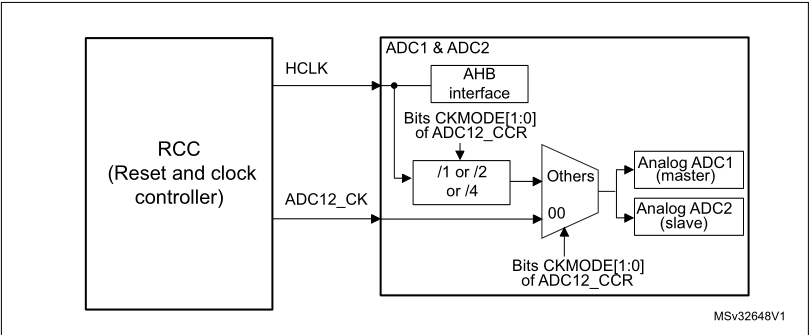
The ADC clock source is essentially the choice between a synchronous (AHB- or APB-derived) or asynchronous (independent from clock-domain resynchronizations). Generally picking the asynchronous source is a safe option, e.g. for STM32F0 by setting the value for CKMODE in ADC_CFGR2 and enabling the high-speed ADC clock (here the 14 MHz HSI clock):
ADC1->CFGR2 &= ~ADC_CFGR2_CKMODE;
RCC->CR2 |= RCC_CR2_HSI14ON;
while ((RCC->CR2 & RCC_CR2_HSI14RDY) == 0) { }
Of importance here is to wait for the clock source to stabilize before we proceed. With the HSI14 clock on F0 this is done by waiting for the HSI14RDY bit to be set in RCC_CR2.
Using a synchronous, bus-derived clock mode is also an option, e.g. the AHB clock without divider on F334 MCUs:
ADC1_2_COMMON_BASE->CCR |= ADC_CCR_CKMODE_1;
With the clock mode selected and the previous tasks also crossed off the list, we can proceed to the configuration of the channels we wish to sample during a sequence.
Channel Configuration

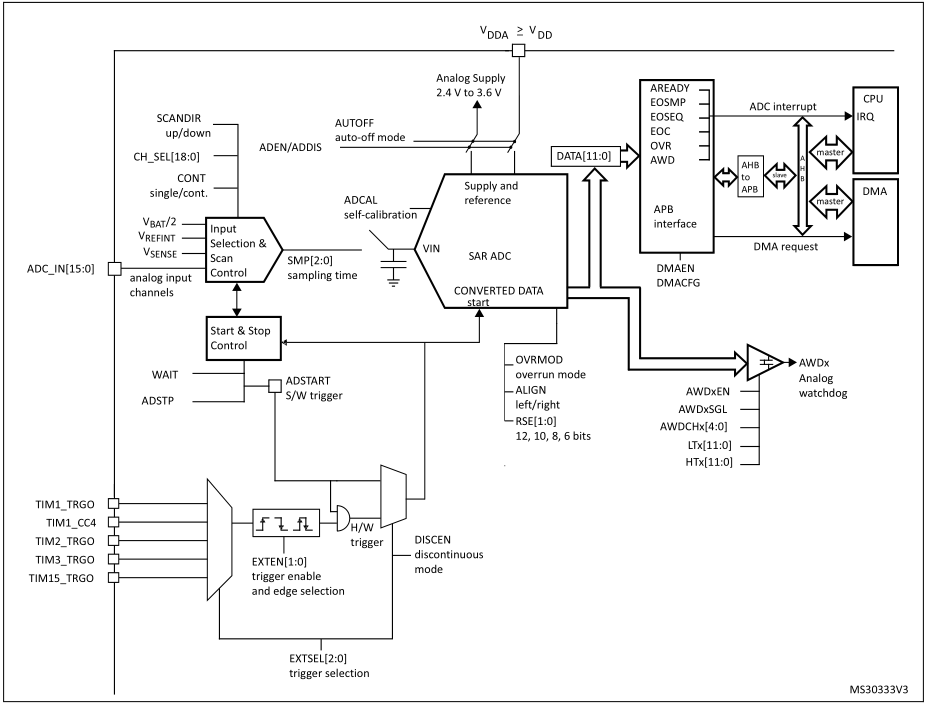
Each ADC is connected to a number of analog input channels, with a range of fixed external (GPIO-connected) channels, and an additional number of so-called internal channels. These latter channels are connected to the internal temperature sensor (Vsense), internal voltage reference (Vrefint), battery voltage (Vbat), and on the F334 MCUs there is Vopamp2 on channel 17 of its second ADC peripheral for an embedded operational amplifier.
The way a channel is configured is where the ADCs of the F0 and F3 families begin to diverge significantly. If we look at F0, configuring ADC1’s channels is performed by setting the channel as active in ADC_CHSELR, followed by the setting the sample time. If we configure channels 1 (GPIO) and 16 (Vsense), for example, we get:
ADC_BASE->CCR |= ADC_CCR_TSEN;
ADC1->CHSELR |= (1 << 1);
ADC1->CHSELR |= (1 << 16);
ADC1->SMPR = 7;
This sets channels 1 and 16 as active in the channel selection register, and sets the sample time to the maximum length (0b111). For channel 16 (Vsense), this is the recommended sampling length for sampling Vsense (239.5 ADC cycles). As the sampling time on F0 ADCs is the same for all channels, we have to pick the longest required sampling time here.
Note that we also have to enable the TSEN bit in the common ADC_CCR register in order to enable this channel. The same is true for the other internal channels, using the VREFINT and VBAT bits in the same register. Finally, note that we have to enable the analog mode on the GPIO pin we wish to use for analog input.
Next, let’s look at what configuring the same channels looks like on an F334 device:
ADC1_2_COMMON_BASE->CCR |= ADC_CCR_TSEN;
ADC1->SQR1 = 1;
ADC1->SQR1 |= (1 << 6);
ADC1->SQR2 |= (16 << (6 * 2));
ADC1->SMPR2 |= (7 << (3 * 6));
Here too we have to enable the TSEN bit, but the way a sampling sequence is set up is more complicated. Basically the SQR1 through SQR4 registers contain the successive channel numbers to be sampled in the sequence, with the first entry in ADC_SQR1 containing the number of channels in the entire sequence (with 0 meaning one channel).
With the channels configured as such using otherwise the default settings, we are ready to start the sequence.
Running A Sequence
Before we can start a sequence, we wish to make sure that ADRDY in the ADC_ISR register is 0. This lets us know that we can safely start a new sequence. Next, we enable the device by setting ADEN in the ADC_CR register for the target ADC peripheral. The device is now ready for the sequencing start.
When we write to the ADSTART bit of the ADC_CR register, it causes the ADC to begin sampling, which by default is as a single sequence, meaning that it will sample each active channel once, before stopping. When a channel has been sampled, we can detect this by waiting for the EOC (End Of Conversion) bit in the ADC_CR register to be set. Once this bit becomes a ‘1’, we can read the sampled value from the ADC_DR register, which will reset the EOC bit. Once the entire sequence is complete, EOSEQ in ADC_ISR will be set.
Handling Sampled Values
The sampled value will be a number between 0 and the maximum bit value: 4095 in the 12-bit case. This makes it easy to detect the state of an external potentiometer, which will output voltages that span the full range. If you want to know exactly what voltage is being output, you need to do some scaling. For example, if you are supplying the ADC with 3.3 V, a reading of 1337 is 1337 / 4095 * 3.3 V = 1.077 V in the real world.
The internal temperature sensor works similarly, but requires calibration from voltage to temperature, or you can just take “typical” values from the data sheet. For the F042 MCU these are 0x1FFFF7B8 for 30°C and 0x1FFFF7C2 for 110°C. We take the 12-bit value we got for Vsense as the raw temperature (in an int16_t variable) and plug it into the formula given in the reference manual:
int32_t temperature = 0;
temperature = (((int16_t) raw) - *TEMP30_CAL_ADDR);
temperature = temperature * (int32_t)(110 - 30);
temperature = temperature / (int32_t)(*TEMP110_CAL_ADDR - *TEMP30_CAL_ADDR);
temperature = temperature + 30;
For the referenced STM32F042 MCU, this gives a temperature of around 36°C shortly after writing the firmware image to the device, with a room temperature of about 28°C. While the internal temperature sensor of STM32 devices are not guaranteed to be very accurate, using the provided calibration values it should be accurate to within a few degrees, and certainly enough for relative temperature measurements, which is enough to figure out if the chip is overheating.
Only The Beginning
The preceding gives only a brief introduction to the ADC peripherals as they exist within STM32 MCUs, of course. We only used a single ADC, and left the sampling resolution, data alignment, etc. at their defaults. These options we will look at in more detail in an upcoming article, along with the use of interrupts, continuous mode and the multi-mode operation of multi-ADC F3 MCUs.
Regardless, it should be possible to perform many essential ADC-related tasks with the information provided so far, and to understand some of the fundamentals behind their operation.


Great tutorial! Looking forward to future installments. This is why I visit Hackaday daily.
+1
Great tutorial thanks! Looking forward to the follow-up. :) Any chance of a follow-up concerning best practices for minimizing noise/jitter? Things like turning off adjacent peripherals during the sampling period? How about supersampling?
You should touch on the input impedance at different sampling speeds. You can find a formula for the input impedance in the stm32 datashee. The input impedance is much lower at higher frequencies and can potentially affect your readings on things like resistor dividers or temperature sensors. This can be mitigated with opamps or even just capacitors at the analog input if the signal is infrequently sampled.
Nice and simple intro to ADC on STM32.
Bare-Metal Unobtainium
exactly, since years back, new STM32 devices exists in a quantum state.
Two corrections:
First, the minor one. The calibration actually calculates the offset and corrects for that, it isn’t simply applying a value measured at manufacture. In fact it is recommended to re-run calibration if certain conditions change, particularly the analog supply voltage. As said, a minor correction.
Now for the major correction. The output sample value is always between 0 and 4095 (for a 12-bit ADC reading), and has absolutely nothing to do with millivolts – it’s the numerator of a fraction. 4095 roughly corresponds to VDDA, so probably about 3.3 V. As an example, a reading of 2048 corresponds to a voltage of about 1.65 V. Or as a formula:
Vin = VDDA x ADC_DR/4096
This is correct, and now fixed in the text.
Helpful Tutorial thankyou.
Came across this in the datasheet:
Bit 0 ADRDY: ADC ready
This bit is set by hardware after the ADC has been enabled (ADEN = 1) and when the ADC reaches a state where it is ready to accept conversion requests.
This suggests you should enable the ADC first, and then check ADC_ISR_ADRDY
Hi, I am trying to BM program my NucleoG431 board. I follow very similar steps that you explained above. However could not get the any result except from “0” at the data register of ADC. Can you help me out If I send my code to you? Thanks in advance.