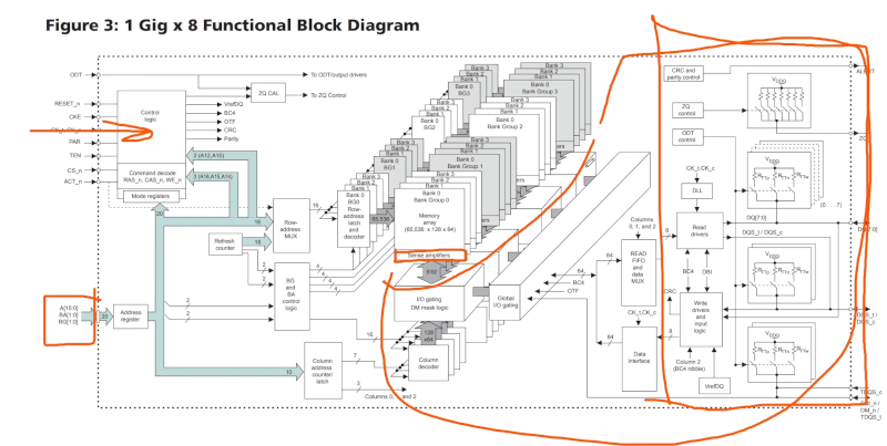
One of the problems with being engaged in our hobby or profession is that people assume if you can build a computer out of chips, you must know all the details of their latest laptop computer. Most of the memory we deal with is pretty simple compared to DDR4 memory and if you’ve ever tried tweaking your memory, you know a good BIOS has dozens of settings for memory. [Actually Hardcore Overclocking] has a great description of a typical DDR4 datasheet and you can watch it in the video below.
Of course, he points out that knowing all this really doesn’t help you much with memory overclocking because you can’t really predict the complex effects without trial and error. However, most of us like to understand the knobs we are randomly twisting. On top of that, one theme of the video is that DRAM is dumb and simple. If you’ve ever thought about using it in a project, this might be a good place to start.
After all, there are only 18 commands — way less than a typical microcontroller. If self-design appeals to you, you’ll be a little disappointed that he doesn’t cover the self-refresh and power saving modes, but the video will give you a good foundation to start learning more.
Even of the 18 commands, to just read and write, you only need a small number of commands. However, if you want to roll your own, you’ll need quite a few of them. If you are targeting an FPGA, there are a number of FPGA-based controllers like this one that can help you learn even more.
Don’t forget that DDR5 is going to make you buy new RAM soon enough and then you’ll have lots of spare DDR4. Of course, these days you might prefer designing around NVMe which is sort of memory and sort of a disk drive.


Low capacitance on lines for good slew rate
Differential traces as close as possible
Length matched traces (impedance matched if its very high speed)
Line termination resistors
Am I missing anything?
HBM2 and directly connecting the RAM to a processing unit via interposer on the same package substrate. Radeon VII quite is something to ogle.
Nice to ogle if one wants PCIe 3.0
explain how is PCIe 3.0 limiting at 16x lanes…
too bad they seem to be kicking the bucket because of the connections between the interposer failing…
By the time they fail, it’s time for a new generation.
Just my luck; Just in time for me to finish writing the text of my Master’s thesis. I had a go at writing my own PHY and controller for DDR3 SDRAM, so I had to churn through the JEDEC standard and part datasheets myself.
I’ve often wondered if any of the various PC RAMs that have been & gone are usable with a microcontroller – there’s a few projects where a cheap gigabyte or four of RAM coupled with a mid-level micro would open up some possibilities.
If the chip supports it, sure. The problem, though, with DDR SDRAM isn’t so much in the logic required to drive it, it’s primarily in the physical interface and the clocking to the chip. This goes from the SERDES units in the controller (be it a microcontroller, an FPGA, or a purpose-built DDR SDRAM controller IC, if those exist at all?) to the physical layout of the parts on the PCB. Traces should be treated as transmission lines, because the frequencies are ludicrous (300+ MHz for DDR3), and they need to be length and impedance matched.
Though you’d be hard pressed to actually write the logic with a generic microprocessor. You need complete determinism down to one clock period, so at 300 MHz that’s 3.33 ns. That alone is a tall order, even assuming the uC you’re employing has a proper PHY layer.
You can’t even write your own PHY layer on a Xilinx 7 series FPGA (which has SERDES and IDELAY primitives readily available), so this has to be baked into the chip you’re using (Xilinx offers the functionality through the MIG IP — I think some microcontroller vendors offer similar IPs for their chips).