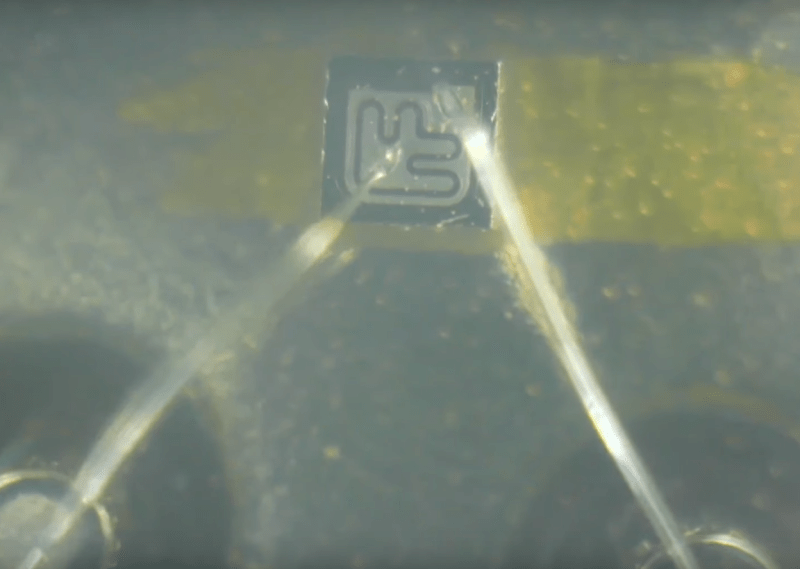
Building things in a lab is easy, at least when compared to scaling up for mass production. That’s why there are so many articles about fusion being right around the corner, or battery technology that’ll allow aviation to switch away from fossil fuels, or any number of other miraculous solutions that never come into being. They simply don’t scale or can’t be manufactured in a cost effective way. But even when they are miraculous and can be produced on a massive scale, as is the case for things like transistors, there are some oddities that come up as a result of the process of making so many. This video goes into some of the intricacies of a bipolar junction transistor (BJT) and why it looks the way it does.
The BJT in this video is a fairly standard NPN type, with three layers of silicon acting as emitter, base, and collector. Typically when learning about electronics devices the drawings of them are simplified two-dimensional block diagrams, but under a microscope this transistor at first appears nothing like the models shown in the textbook. Instead it resembles more of a bird’s foot with a few small wires attached. The bird’s foot shape is a result of attempting to lower the undesirable resistances of the device and improve its performance, and some of its other quirks are due to the manufacturing process. That process starts with a much larger layer of doped silicon that will eventually become the collector, and then the other two, much smaller, layers of the transistor deposited on top of the collector. This also explains while it looks like there are only two layers upon first glance, and also shows that the horizontal diagram used to model the device is actually positioned vertically in the real world.
For most of the processes in our daily lives, the transistor has largely been abstracted away. We don’t have to think about them in a computer that much anymore, and unless work is being done on high-wattage power electronics devices, radios, or audio amplifiers it’s not likely that an average person will run into a transistor. But this video goes a long way to explaining the basics of one of the fundamental building blocks of the modern world for those willing to take a dive into the physics. Take a look at this video as well for an intuitive explanation of the close cousin of the BJT, the field-effect transistor.


Dr. Bergstrom spends what seems like a full minute with his head blocking the portion of the whiteboard he’s describing.
The American 2N2222 transistor with its “star architecture” is also interesting, I think.
It had ab unusual shape, too.
http://www.semiconductormuseum.com/Transistors/Motorola/Haenichen/Haenichen_Page12.htm
In a pinch an side cutter enabled uncapped unit acts as a simple phototransistor.
Good thing his area of expertise is transistor design and not video production! 🤣🤣
Thanks for this. Brings me back to earlier days. Transistors are taken for granted now. Most people have no idea how IC’s are made in a foundry.
To be honest, I hardly value transistors, either.
They killed off the Nuvistors, which were more sophisticated and a miracle of human engineering.
If transistors hadn’t been, nano tubes had been developed instead. Their maximum frequency can be much higher than that of transistors.
Also, transistors are hardly ingenious. They’re based on the crystal detector, a 19th century technology.
The only transistor that truly was remarkable was the field-effect-transistor.
It essentially emulates the functionality of a thermionic valve.
Anyway, it’s hard to think different these days because of our dependence and addiction of the technology.
Just look at the smartphone. Seemingly everyone mentions it as the greatest invention, ever.
But in reality, it’s nothing but a PDA with a cellphone modem tacked on.
The smartphone also ruined the traditional, PC-oriented internet.
If only the iPhone never had been.
Just look at Japanese internet, the people there still use full-size websites that provide loads of information, like it was in the 90s/early 2000s.
Not the minimalist internet experience we do have now in the western world. *sigh*
I don’t really mind “smartphones”, as you say it’s basically a pda with internet. Ofcourse everyone wants to have a computer in their pocket!
What I don’t get is how and why on earth most people seem to think that such a small computer could replace a proper computer experience?
Having a good screen, keyboard etc is such a vastly better and faster way to use a computer.
So how could anyone not also have a computer set up at home?
According to one of my mentors, the Nuvistor was two years too late. He was a lead on the project at RCA. They really tried to push the vaccum tube technology as hard and fast as they could, but the planar process effectively leapfrogged past. RCA, which had previously placed its bets on vacuum tube technology had to quickly ramp up its solid-state efforts–and did, much to their credit. The Overlay Transistor, COSMOS, the LCD display was all theirs–then like so many others, gave its all away….
You can’t make a Nuvistor as small as a transistor. Integrated Nuvistor circuits are right out.
The ancient and decrepit 555 timer IC has over 20 transistors. A Nuvistor equivalent would be huge.
https://en.wikipedia.org/wiki/555_timer_IC
The transistor was more important and useful than the Nuvistor – however cool the Nuvistor itself might be.
Well, for a video just under 12 minutes, its not Hollywood, but I thought the Dr properly answered the question and provided the process information needed to comprehend the topic. Good direct answer, no fluff.
That gold-ish smear the Dr called “leadframe” looks more like the attachment material itself. The 2N2222 was typically diebonded to its TO-18 enclosure with Au/Sn solder , eutectic Au/Si scrubbing or similar methods. The leadframe mounting method came later with TO-92 and the like.
To probe further try: 1) https://www.richis-lab.de/ and 2) https://zeptobars.com/en/