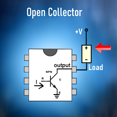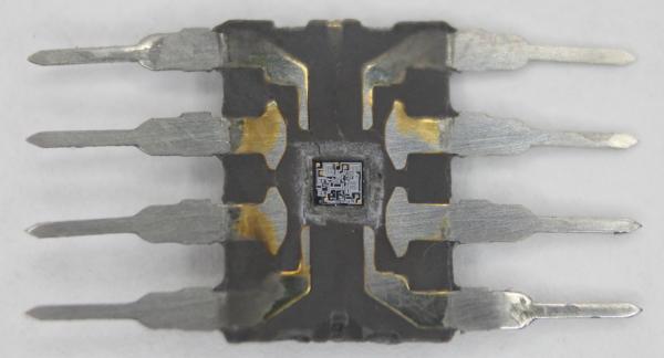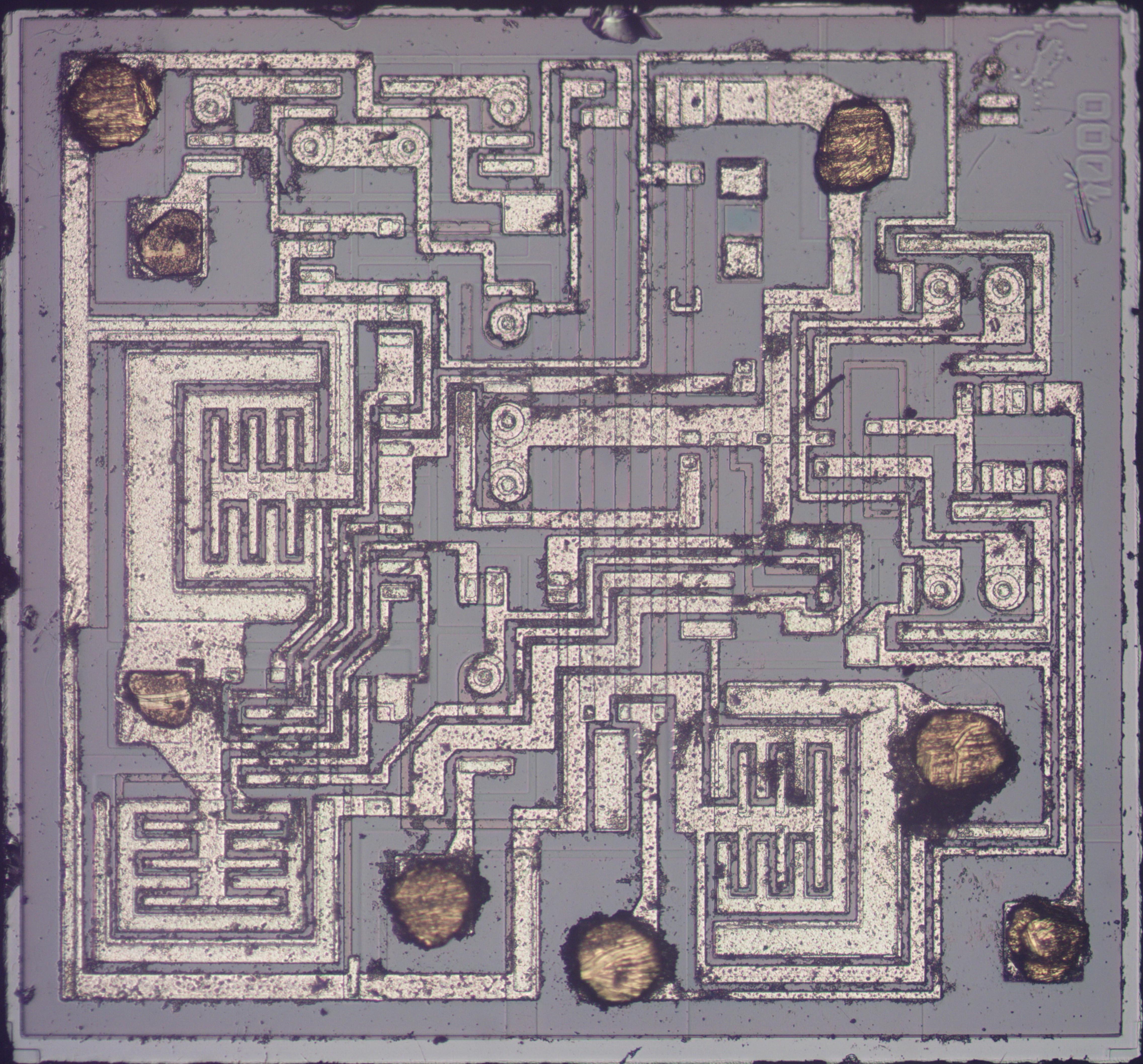
For the Component Abuse Challenge our hacker [Tim Williams] observes that N-P-N reads the same way forwards and backwards, so… what happens if we reverse bias one? (Note: this remark about N-P-N reading the same forward and backward is a lighthearted joke; in fact the level of doping in the emitter and collector is different so those Ns are not fungible and will exhibit different properties and have different characteristics.)
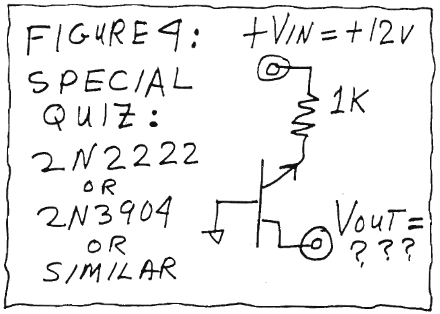 In the margin you can see how the question was originally posed by Bob Pease back in March 18, 1996.
In his article [Tim] mentions that some transistors are specifically designed to operate when reverse biased, which [Tim] calls “inverted mode”, whereas most transistors are not designed to work in this fashion and that’s the sort of abuse that could damage the component and lead it to malfunction.
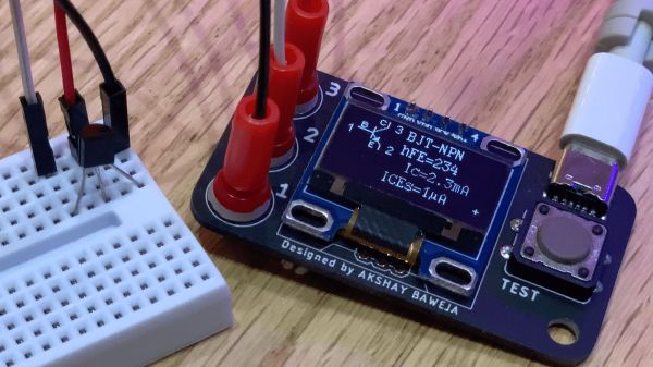
But what is Vout? [Tim] reports that he measured approximately -0.4 volts using his high-impedance meter. We tried this experiment in the lab ourselves but we were not able to duplicate [Tim]’s result; however there is a long list of potential reasons for such an outcome. If you do this experiment yourself we would love to hear about your results in the comments section!
If you’re still learning about transistors you might like to check out our five part series on transistors as amplifiers, starting here: Won’t Somebody, Please, Think Of The Transistors!
Thanks to [Tim] for his submission, we wish him the best of luck in the competition!