What’s solder for, anyway? It’s just the stuff that sticks the parts to the PCB. If you’re rapid prototyping, possibly with expensive components, and want to be able to remove chips from the board easily when you spin up the next iteration, it would be great if you didn’t have to de-solder them to move on. If only you could hold the parts without the solder…
That’s exactly the goal behind [Zeyu Yan] et al’s SolderlessPCB, which uses custom 3D printed plastic covers to do the holding. And it has the knock-on benefit of serving as a simple case.
In their paper, they document some clever topologies to make sure that the parts are held down firmly to the board, with the majority of the force coming from screws. We especially like the little hold-down wings for use with SMD capacitors or resistors, although we could absolutely see saving the technique exclusively for the more high value components to simplify design work on the 3DP frame. Still, with the ability to automatically generate 3D models of the board, parts included, this should be something that can be automated away.
The group is doing this with SLA 3D printing, and we imagine that the resolution is important. You could try it with an FDM printer, though. Let us know if you do!
This is the same research group that is responsible for the laser-cut sheet-PCB origami. There’s clearly some creative thinking going on over there.


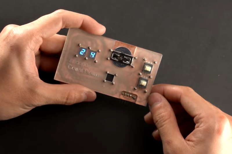
Pretty nice – and the holes for component alignment could simplify SMD use for people who find it too fiddly to solder them.
So one has to machine or print a specific cover to hold the components and make *some* contact.
So any change in the schematics leads to machining and printing another cover, and likely another circuit boards,
what is the benefit in that ? I cannot see any : it´s way more tedious, cumbersome, time-consuming, and makes only so-so contacts. Good luck debugging anything …
They could use a memory foam substance. That has a fire proof film on the side that touches the circuitry. Totally could be used again.
Printing it really isn’t that much of an issue, just make the cover when you send off the new PCB design and then you can just print it and have it ready for when the board arrives.
Printing a cover using a largely automated process is much less tedious and time consuming than trying to desolder a component and then solder it to the new board, especially if you are using high pin count components.
Note that this is meant for changing PCB designs, so your comment about needing to get another circuit board made is pretty irrelevant since the alternative is to get the new PCB and take components off of the old one to put on the new one. The difference with this is that you just need to print a new cover, you don’t need to deal with desoldering and resoldering components.
As for debugging, if done well this shouldn’t be any worse than using removable brackets or clamps for holding components.
I agree, seems way too easy to mistake a weak connection for another issue and have a guy chasing his tail when if he’d only pushed down in the right spot, his design might have worked flawlessly….
Funny how people often say “I don’t want to be…” and then go on exactly doing that ;)
For me it’s just a demonstration of a novel concept which might be useful in some usecases. This one could be for electronics kits for people (/kids ?) without soldering gear. See it as a proof of concept and store it in your brain and you even might reach back to that some time in the future.
It is interesting, but for me, the concept is killed by the lack of access to the circuit, as pointed out by paulvdh. It’s a prototype. Even if it works first time (yeah, right) you still need to be able to probe things to confirm your designed tolerances.
I guess you could add additional test connectors/points, but in my experience the traces I need to probe rarely seem to match up with my carefully added test points, so I inevitably need to pull out component pins directly.
It may be possible to design it in such a way that component pins are still accessible. I would think that it should be possible for at least small and simple components, like surface mount resistors or capacitors, just leave holes that go down to the component contacts.
A solution in dire need of a problem.
I see one practical use for this: a rig for programming SMD microcontrollers or for testing SMD components.
Yes that could be quite useful. Also using BGA packages without having to solder them. Though I’m not sure how to get the alignment just right, or if all the balls will make adequate contact with the pads (given the density)
I think the alignment is intended to just take care of itself. The boards and the housings are all made locally, so you can probably refine the procedure until it works to your tolerances?
You’d have to try it out to be sure. And probably refine it a couple times as well. But it’s a cool idea.
please make arduboy and show it working or not?
What does it solve?
Not time, because it’s faster to solder components directly than to save little time mounting them with this jig and then wasting 100x more debugging.
Not cost, because most components are cheap and you waste time (=money) debugging.
Not landfill, because these positioning covers take more space than components and are disposable on any minor revision vs a prototype soldered pcb revision you can make minor fixes with knyar wire or soldering components in a makeshift way.
Hewlett-Packard did this a long time ago.
https://www.hpmuseum.org/tech30.htm
> Hewlett-Packard did this a long time ago.
Yes. And I had to solder my one later because it did not relay work. .-)
Olaf
Ditto , the display connection was endlessly dodgy.
In the long run it was relying on an elastomeric foam for contact pressure, and that is guaranteed expiry date.
Sun Microsystems used pressed pin technology to secure parts to back and centre planes. They claimed it improved connectivity.
SGI used compression connections instead of card edge slots for their XIO bus. When new it made motherboard and expansion boards an easy and tool-less swap. However, a speck of dust or a fingerprint was enough to cause problems.
How about using this to create a test jig for your 555’s
What does it solve?
Not time, because it’s faster to solder components directly than to save little time mounting them with this jig and then wasting 100x more debugging.
Not cost, because most components are cheap and you waste time (=money) debugging.
Not landfill, because these positioning covers take more space than components and are disposable on any minor revision vs a prototype soldered pcb revision you can make minor fixes with knyar wire or soldering components in a makeshift way.
Is it actually unreliable? Everyone says it is, but I wouldn’t be surprised if it’s at least vaguely acceptable. Soldering is by far the hardest part of most anything electronic, up until the “you need calculus for the PCB design” level, unless you’re very, very good with your hands, so I can see this or a version of this having real value.
This could also be very useful for trying out components. By using this you would have the ability to swap out components and test them as you need to, so you could try multiple resistor or capacitor values or potentially even different diodes or mosfets.
Some NASA level engineering being proposed here!
Perhaps you should aspire to better then ‘trial and error’ circuit design?
I do get that everybody has to start somewhere.
100 in 1 kits used springs to hold wires.
There is another bad idea on hackaday right now for a replacement for protoboards.
You need to solder more.
Also: Calculus is hard? WTF? It’s pretty basic math. High schoolers take calc.
(Calc/diffeq/control theory) is for circuit design BTW. Only after that is done do you layout the board.
Soldering is the easy part, like coding is the easy part of software.
Debugging is _always_ the bitch.
Everybody that says this is unreliable has debugged a badly soldered board with a few pins just in contact (often soldered but cracked). They are intermittent. Sometimes very, sometimes slightly. Tiny capacitors everywhere. Thermal flex is fun!
This is fine, but for a moment I thought we were talking about something I’ve wondered about in the past: could components be mounted using friction welding?
What I picture is basically a pick-and-place robot, but as it places the components it vibrates them to weld the leads onto the pads. I don’t know that there’d be much benefit for mass production, but it might be good for desktop prototyping.
I’m not likely to try this myself, but it could be a cool project if it’s remotely viable.
(Posturing aside, plenty of normal, decent people are interested in ways to avoid soldering, especially of surface mount components)
I don’t know if that would work, but maybe as test rig one of the larger “bristle blocks” (Stickle Bricks?) with pogo pins stuck between the bristles. Hopefully the bristles are packed densely enough that 1. the pins would not fall off, and 2. there’s enough precision to get the pogo pins aligned with the test pads. Then clamp the whole thing down onto the circuit board for good contact.
HP did similar with their Series 30 calculators around 1978, though not with bolts. The had a frame that went around the ICs, and the frame, PCB, and a rigid backboard were clamped at the edges. They got a US patent on their technique.
Unfortunately it was not reliable over time, and they switched production to conventional soldered construction.
This new techniques seems likely to have better reliability, since the clamping is closer to the components. There’s less moment arm so less opportunity for flex.
All the folks saying this is pointless, I think this isn’t necessary aimed at hackers particularly, because for most use cases it really is pointless. One really good use I could see for it would be when you have something expensive and experimental that you only have a small amount (maybe one) of and you want to reuse it without soldering and desoldering over and over and potentially damaging it. Or even for extremely heat sensitive components that might prefer not to be soldered.
Isn’t this what sockets were for?
I don’t know if anyone else with RF experience actually read the paper, but their network analysis characterization seems really badly done – it’s clear someone lent them a fancy VNA, but didn’t provide any help designing the characterization artifacts or interpreting the data.