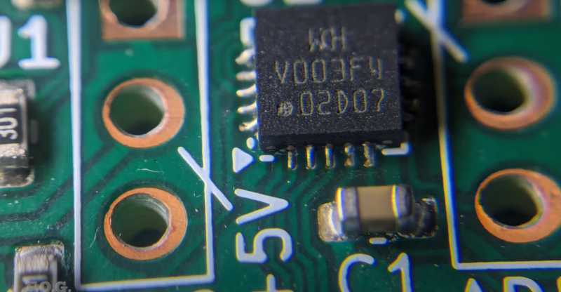
Now before you start asking yourself “best for what purpose?”, just have a look at the quality of the DIY PCB in the image above. [ForOurGood] is getting higher resolution on the silkscreen than we’ve seen in production boards. Heck, he’s got silkscreen and soldermask at all on a DIY board, so it’s definitely better than what we’re producing at home.
The cost here is mostly time and complexity. This video demonstrating the method is almost three hours long, so you’re absolutely going to want to skip around, and we’ve got some relevant timestamps for you. The main tools required are a cheap 3018-style CNC mill with both a drill and a diode laser head, and a number of UV curing resins, a heat plate, and some etchant.
[ForOurGood] first cleans and covers the entire board with soldermask. A clever recurring theme here is the use of silkscreens and a squeegee to spread the layer uniformly. After that, a laser removes the mask and he etches the board. He then applies another layer of UV soldermask and a UV-curing silkscreen ink. This is baked, selectively exposed with the laser head again, and then he cleans the unexposed bits off.
In the last steps, the laser clears out the copper of the second soldermask layer, and the holes are drilled. An alignment jig makes sure that the drill holes go in exactly the right place when swapping between laser and drill toolheads – it’s been all laser up to now. He does a final swap back to the laser to etch additional informational layers on the back of the board, and creates a solder stencil to boot.
This is hands-down the most complete DIY PCB manufacturing process we’ve seen, and the results speak for themselves. We would cut about half of the corners here ourselves. Heck, if you do single-sided SMT boards, you could probably get away with just the first soldermask, laser clearing, and etching step, which would remove most of the heavy registration requirements and about 2/3 of the time. But if it really needs to look more professional than the professionals, this video demonstrates how you can get there in your own home, on a surprisingly reasonable budget.
This puts even our best toner transfer attempts to shame. We’re ordering UV cure soldermask right now.


Nowhere near as pretty as these boards but I make my SS boards by milling then flipping over and using the laser for black silkscreen. Alignment is not critical because it’s just labels. The trick is to spray the component side of the blanks white beforehand.
No plated through holes. That’s a big downside, especially because professionally made PCBs are so cheap and fast these days.
Yep. If you wanted to have them, you’d start by drilling the holes first – but then the whole process goes belly up because the holes would fill up with the UV resin.
I don’t know how long it takes for your area and what you consider fast but I do simple one sided PCBs for 0.4mm pitch ICs under a hour in a flat (no garage or a lab with nicely pre-prepared tools) with 2 to 10€ boards with UV resist preaplied which I have from a shop 15min by car.
Whereas JLCPCB takes whole f’ing days!
Can you explain your process in more detail. What tool do you use to pattern the boards? What chemicals do you use to wash away the unexposed resist? What do you use to etch the copper?
You can use a SLA printer to expose you pattern on it. I made some experiments to electrochemically cut thin sheet metal where i modified a cheap SLA printer to have calibrated end stops and a UV clear carrier plate with notches for these end stops.
Then i could mount the board with some tape on one side of the carrier just flip the board and have front an back aligned. I also calibrated the scale of the STL i needed to export using Vernier patterns to know how off I am to the desired dimension and could easily measure differences below .1mm.
Sodium carbonate solution to wash the unexposed parts (or exposed parts if you use the other kind of uv-resist).
To dispose the liquids you can use cat litter as the problem is mostly with liquid consumables.
Up to the actual etching process it all worked great, but I was not able to get a uniform etching. And not wanting to handle highly corrosive substances under high pressure as
a proven recipe, this project got laid on ice.
I use KiCad for designing.
Then I used to print it on a transparent foil using an old laser printer (literally from 1990) but even with a fresh toner I had to always print it 3 times then overlay the prints and secure them using a drop of CA glue. Then I peeled off a protective opaque film from a PCB like this t.ly/u74wg overlayed it with the printed foils and a piece of glass (ordinary glass plate from a broken scanner) and placed a nail polish hardener thingy (has UV lamps) on top and let it shine for 2 minutes. This used to be the longest and work intensive manufacturing phase (i.e. not counting designing in KiCad). I bought a new Creality Halot One MSLA printer for 150e just for this two years ago but haven’t tried it yet since I’m working on non-PCB parts of my forever projects currently.
Photo development phase: Wash it in 1.5% NaOH water solution for a few seconds.. agitate it by shaking it with a gloved hand.
Etching phase: Put a very hot water in a big tupperware container and place small tuperware container with FeCl3 inside it. With gloved hand hold the PCB inside it Cu side facing down, shake it a little.. for 15-30minutes while reading HaD…
Drill, solder, optionally spray it with protective coating at the end but don’t forget to cover all connectors :D
When etching takes too long I take the FeCl3 bottle (or more like CuCl2) to a public collection facility and but a new one.
I couldn’t be less interested in doing this myself (I’ve got ridiculous rabbit holes of my own), but I love reading about the hobby rabbit holes other hackaday readers go down, and a detailed build guide is always invaluable!
‘facing down, shake it a little.. for 15-30minutes while reading HaD…’
Kinky!
Exactly my thought. If your hobby is making PCBs, then this video is very impressive. On the other hand, if electronics is your hobby maybe order em.
Personally, I have plenty of other projects to work on while I wait for my 6mil trace-n-space 6-layer PCBs with 154 plated holes,3mil mask slivers, ENIG finish, electrically tested…My time is worth more than the $10.
That’s me too, but I have plenty of things I shouldn’t waste my time doing either that take up more than half of my hobby time! I am a sucker for getting my pcbs with passives assembled nowadays, it just saves so much time, and I’ve proven to myself I can do it (down to 0402, at least).
Yeah, PCBA is getting to the point where it’s just more cost-effective (ie charging my hobby time at the rate my work time would pay me for) just to have JLCPCB put all the parts on themselves. Like you said, I’ve proved I can assemble them myself, it’s just not the fun part of the hobby for me. And I still get to do the exciting rework bits when my design isn’t quite right. :)
“Personally, I have plenty of other projects to work on while I wait for my 6mil trace-n-space 6-layer”
Finding a dumbass mistake in a section of a 6-layer design you haven’t done before saves a ton of time. Although in that case, I don’t really care about making it pretty.
A lot can be done with a single side and some jumper wires. But I would probably just mill the traces, the extra accuracy from etching is not that much.
You can use copper rivets for that.
https://fab.cba.mit.edu/classes/863.16/doc/tutorials/PCB_Rivets/
The only thing you *actually* need plated through-holes for are vias, since actual through-hole parts you can just solder both sides if you need to. So yeah, rivets are fine.
The only thing is you need to remember you can’t drop a via under a component with rivets since it won’t be flat. In that case, you can thread a thin bare wire through, solder it to both sides, and flush-cut it. Bit of a pain to make sure it works, but if it’s only for a prototype or something, not a big deal.
This project is FANTASTIC!
But why discount the “for what?” question?
That question is always the most important.
If that isn’t your first question, every single time you hear the word “best”, then you are doing it wrong and can’t be trusted to have an opinion.
Qualify EVERYTHING.
+1 – after too many unfinished projects in the drawer and programming challenges in need for more work (looking at you, advent of code!), I feel like “for what?” helps keeping me from jumping from one task to the next.
The silk screen gorgeous. I wonder if that method could be used to make a labelled front panel, eg old skool white writing on black.
I don’t see why not. This is a type of UV printing and should work for any flat material, not just PCBs. You need the right UV ink for the material and you might need to pretreat, but it should be possible to use this process to make custom graphics on an aluminum front panel, for instance.
Nah. Even if the PCBs take 60 days to come to my hands in Brazil, it is worth the while
Wow, this is incredibly impressive for in house results! Dang!
When we got boards with off center drilling like this we rejected them. They were not properly connected most likely to lower layers, which were possibly power and ground on 4 layer boards, and maybe clipping traces if more with inter layer signals. I know this is about a DIY technique, but it wouldn’t work at the scale we were running at 500 to 1000 boards a week. I would look at every board as part of my acceptance test and stamp them after looking with magnification at 4 corners and center as well as selectively checking for shorts on power / ground. These sort of boards usually had more power shorts than others sent in. The ground and power plane filled the entire layer with cutouts for the vias, and off center like this would usually nick those inner layers